DF2437FV Renesas Electronics America, DF2437FV Datasheet - Page 767
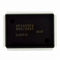
DF2437FV
Manufacturer Part Number
DF2437FV
Description
IC H8S/2437 MCU FLASH 128QFP
Manufacturer
Renesas Electronics America
Series
H8® H8S/2400r
Specifications of DF2437FV
Core Processor
H8S/2600
Core Size
16-Bit
Speed
20MHz
Connectivity
I²C, SCI
Peripherals
POR, PWM, WDT
Number Of I /o
85
Program Memory Size
256KB (256K x 8)
Program Memory Type
FLASH
Ram Size
16K x 8
Voltage - Supply (vcc/vdd)
3 V ~ 3.6 V
Data Converters
A/D 16x10b
Oscillator Type
Internal
Operating Temperature
-20°C ~ 75°C
Package / Case
128-QFP
Lead Free Status / RoHS Status
Lead free / RoHS Compliant
Eeprom Size
-
Available stocks
Company
Part Number
Manufacturer
Quantity
Price
Company:

Part Number:
DF2437FV
Manufacturer:
Renesas Electronics America
Quantity:
10 000


14-Bit PWM Timer (PWMX) ................. 233
16-Bit Count Mode ................................. 298
16-Bit Free-Running Timer (FRT) ......... 247
16-Bit Timer Pulse Unit (TPU)............... 309
16-Bit, 2-State Access Space .................. 109
16-Bit, 3-State Access Space .................. 112
2fH Modification .................................... 404
8-Bit PWM Timer (PWM)...................... 223
8-Bit Timer (TMR) ................................. 275
8-Bit, 2-State Access Space .................... 107
8-Bit, 3-State Access Space .................... 108
A/D conversion time............................... 539
A/D Converter ........................................ 531
A/D Converter Activation....................... 362
Acknowledge .................................. 497, 515
ADCR ..................................................... 537
ADCR ..................................................... 664
ADCR ..................................................... 676
ADCR ..................................................... 687
ADCSR ................................................... 535
ADCSR ................................................... 664
ADCSR ................................................... 676
ADCSR ................................................... 687
additional pulse....................................... 231
ADDR ............................. 534, 663, 676, 687
Address Space........................................... 22
Addressing Modes .................................... 43
ADI ......................................................... 542
ASTCR ..................................................... 97
Asynchronous Mode............................... 462
Absolute Address.................................. 44
Immediate ............................................. 45
Memory Indirect ................................... 46
Program-Counter Relative .................... 45
Register Direct ...................................... 43
Register Indirect.................................... 43
Register Indirect with Displacement..... 44
Register indirect with post-increment ... 44
Register indirect with pre-decrement.... 44
Index
basic pulse...............................................230
Bcc ......................................................31, 39
bit rate .....................................................456
Boot Mode ..............................................575
BRR ................................ 456, 662, 675, 686
Buffer Operation .....................................346
Carrier frequency ....................................226
Cascaded Connection ..............................298
Cascaded Operation ................................349
CBLANK Output ....................................416
Clamp Waveform Generation .................399
Clear Timing ...........................................426
Clock Pulse Generator ............................637
Clocked Synchronous Mode ...................479
CMIA ......................................................302
CMIA0 ....................................................302
CMIA1 ....................................................302
CMIAX ...................................................302
CMIAY ...................................................302
CMIB ......................................................302
CMIB0 ....................................................302
CMIB1 ....................................................302
CMIBX ...................................................302
CMIBY ...................................................302
Communications Protocol.......................610
Compare-Match Count Mode .................298
Condition Field .........................................42
Condition-Code Register (CCR) ...............26
conversion cycle......................................241
CPU Operating Modes ..............................18
Crystal Oscillator ....................................640
data direction register..............................133
data register .............................................133
Download pass/fail result parameter .......566
Effective Address Extension .....................42
ERI0 ........................................................489
ERI1 ........................................................489
Advanced Mode ....................................20
Normal Mode ........................................18
Rev.2.00 May. 28, 2009 Page 727 of 732
REJ09B0059-0200
Related parts for DF2437FV
Image
Part Number
Description
Manufacturer
Datasheet
Request
R

Part Number:
Description:
KIT STARTER FOR M16C/29
Manufacturer:
Renesas Electronics America
Datasheet:

Part Number:
Description:
KIT STARTER FOR R8C/2D
Manufacturer:
Renesas Electronics America
Datasheet:

Part Number:
Description:
R0K33062P STARTER KIT
Manufacturer:
Renesas Electronics America
Datasheet:

Part Number:
Description:
KIT STARTER FOR R8C/23 E8A
Manufacturer:
Renesas Electronics America
Datasheet:

Part Number:
Description:
KIT STARTER FOR R8C/25
Manufacturer:
Renesas Electronics America
Datasheet:

Part Number:
Description:
KIT STARTER H8S2456 SHARPE DSPLY
Manufacturer:
Renesas Electronics America
Datasheet:

Part Number:
Description:
KIT STARTER FOR R8C38C
Manufacturer:
Renesas Electronics America
Datasheet:

Part Number:
Description:
KIT STARTER FOR R8C35C
Manufacturer:
Renesas Electronics America
Datasheet:

Part Number:
Description:
KIT STARTER FOR R8CL3AC+LCD APPS
Manufacturer:
Renesas Electronics America
Datasheet:
Part Number:
Description:
KIT STARTER FOR RX610
Manufacturer:
Renesas Electronics America
Datasheet:

Part Number:
Description:
KIT STARTER FOR R32C/118
Manufacturer:
Renesas Electronics America
Datasheet:

Part Number:
Description:
KIT DEV RSK-R8C/26-29
Manufacturer:
Renesas Electronics America
Datasheet:

Part Number:
Description:
KIT STARTER FOR SH7124
Manufacturer:
Renesas Electronics America
Datasheet:

Part Number:
Description:
KIT STARTER FOR H8SX/1622
Manufacturer:
Renesas Electronics America
Datasheet:

Part Number:
Description:
KIT DEV FOR SH7203
Manufacturer:
Renesas Electronics America
Datasheet: