DF2437FV Renesas Electronics America, DF2437FV Datasheet - Page 28
DF2437FV
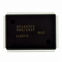
Manufacturer Part Number
DF2437FV
Description
IC H8S/2437 MCU FLASH 128QFP
Manufacturer
Renesas Electronics America
Series
H8® H8S/2400r
Specifications of DF2437FV
Core Processor
H8S/2600
Core Size
16-Bit
Speed
20MHz
Connectivity
I²C, SCI
Peripherals
POR, PWM, WDT
Number Of I /o
85
Program Memory Size
256KB (256K x 8)
Program Memory Type
FLASH
Ram Size
16K x 8
Voltage - Supply (vcc/vdd)
3 V ~ 3.6 V
Data Converters
A/D 16x10b
Oscillator Type
Internal
Operating Temperature
-20°C ~ 75°C
Package / Case
128-QFP
Lead Free Status / RoHS Status
Lead free / RoHS Compliant
Eeprom Size
-
Available stocks
Company
Part Number
Manufacturer
Quantity
Price
Company:

Part Number:
DF2437FV
Manufacturer:
Renesas Electronics America
Quantity:
10 000


Figure 11.14 Conflict between TCNT Write and Increment..................................................... 304
Figure 11.15 Conflict between TCOR Write and Compare-Match........................................... 305
Section 12 16-Bit Timer Pulse Unit (TPU)
Figure 12.1
Figure 12.2
Figure 12.3
Figure 12.4
Figure 12.5
Figure 12.6
Figure 12.7
Figure 12.8
Figure 12.9
Figure 12.10 Example of 0 Output/1 Output Operation............................................................ 341
Figure 12.11 Example of Toggle Output Operation.................................................................. 341
Figure 12.12 Example of Setting Procedure for Input Capture Operation ................................ 342
Figure 12.13 Example of Input Capture Operation ................................................................... 343
Figure 12.14 Example of Synchronous Operation Setting Procedure....................................... 344
Figure 12.15 Example of Synchronous Operation .................................................................... 345
Figure 12.16 Compare Match Buffer Operation ....................................................................... 346
Figure 12.17 Input Capture Buffer Operation ........................................................................... 346
Figure 12.18 Example of Buffer Operation Setting Procedure ................................................. 347
Figure 12.19 Example of Buffer Operation (1) ......................................................................... 347
Figure 12.20 Example of Buffer Operation (2) ......................................................................... 348
Figure 12.21 Cascaded Operation Setting Procedure................................................................ 349
Figure 12.22 Example of Cascaded Operation (1) .................................................................... 350
Figure 12.23 Example of Cascaded Operation (2) .................................................................... 350
Figure 12.24 Example of PWM Mode Setting Procedure......................................................... 352
Figure 12.25 Example of PWM Mode Operation (1)................................................................ 353
Figure 12.26 Example of PWM Mode Operation (2)................................................................ 354
Figure 12.27 Example of PWM Mode Operation (3)................................................................ 355
Figure 12.28 Example of Setting Procedure for Phase Counting Mode.................................... 356
Figure 12.29 Example of Phase Counting Mode 1 Operation................................................... 357
Figure 12.30 Example of Phase Counting Mode 2 Operation................................................... 358
Figure 12.31 Example of Phase Counting Mode 3 Operation................................................... 359
Figure 12.32 Example of Phase Counting Mode 4 Operation................................................... 360
Figure 12.33 Count Timing in Internal Clock Operation .......................................................... 363
Figure 12.34 Count Timing in External Clock Operation ......................................................... 363
Figure 12.35 Output Compare Output Timing .......................................................................... 364
Figure 12.36 Input Capture Input Signal Timing ...................................................................... 364
Figure 12.37 Counter Clear Timing (Compare Match)............................................................. 365
Figure 12.38 Counter Clear Timing (Input Capture)................................................................. 365
Rev.2.00 May. 28, 2009 Page xxvi of xxxviii
REJ09B0059-0200
Block Diagram of TPU ........................................................................................ 310
16-Bit Register Access Operation [Bus Master ↔ TCNT (16 Bits)] .................. 336
8-Bit Register Access Operation [Bus Master ↔ TCR (Upper 8 Bits)] .............. 337
8-Bit Register Access Operation [Bus Master ↔ TMDR (Lower 8 Bits)] .......... 337
8-Bit Register Access Operation [Bus Master ↔ TCR and TMDR (16 Bits)] .... 337
Example of Counter Operation Setting Procedure............................................... 338
Free-Running Counter Operation......................................................................... 339
Periodic Counter Operation ................................................................................. 340
Example of Setting Procedure for Waveform Output by Compare Match .......... 340
Related parts for DF2437FV
Image
Part Number
Description
Manufacturer
Datasheet
Request
R

Part Number:
Description:
KIT STARTER FOR M16C/29
Manufacturer:
Renesas Electronics America
Datasheet:

Part Number:
Description:
KIT STARTER FOR R8C/2D
Manufacturer:
Renesas Electronics America
Datasheet:

Part Number:
Description:
R0K33062P STARTER KIT
Manufacturer:
Renesas Electronics America
Datasheet:

Part Number:
Description:
KIT STARTER FOR R8C/23 E8A
Manufacturer:
Renesas Electronics America
Datasheet:

Part Number:
Description:
KIT STARTER FOR R8C/25
Manufacturer:
Renesas Electronics America
Datasheet:

Part Number:
Description:
KIT STARTER H8S2456 SHARPE DSPLY
Manufacturer:
Renesas Electronics America
Datasheet:

Part Number:
Description:
KIT STARTER FOR R8C38C
Manufacturer:
Renesas Electronics America
Datasheet:

Part Number:
Description:
KIT STARTER FOR R8C35C
Manufacturer:
Renesas Electronics America
Datasheet:

Part Number:
Description:
KIT STARTER FOR R8CL3AC+LCD APPS
Manufacturer:
Renesas Electronics America
Datasheet:
Part Number:
Description:
KIT STARTER FOR RX610
Manufacturer:
Renesas Electronics America
Datasheet:

Part Number:
Description:
KIT STARTER FOR R32C/118
Manufacturer:
Renesas Electronics America
Datasheet:

Part Number:
Description:
KIT DEV RSK-R8C/26-29
Manufacturer:
Renesas Electronics America
Datasheet:

Part Number:
Description:
KIT STARTER FOR SH7124
Manufacturer:
Renesas Electronics America
Datasheet:

Part Number:
Description:
KIT STARTER FOR H8SX/1622
Manufacturer:
Renesas Electronics America
Datasheet:

Part Number:
Description:
KIT DEV FOR SH7203
Manufacturer:
Renesas Electronics America
Datasheet: