DF2437FV Renesas Electronics America, DF2437FV Datasheet - Page 359
DF2437FV
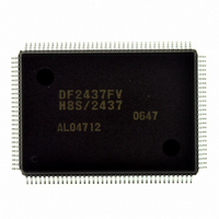
Manufacturer Part Number
DF2437FV
Description
IC H8S/2437 MCU FLASH 128QFP
Manufacturer
Renesas Electronics America
Series
H8® H8S/2400r
Specifications of DF2437FV
Core Processor
H8S/2600
Core Size
16-Bit
Speed
20MHz
Connectivity
I²C, SCI
Peripherals
POR, PWM, WDT
Number Of I /o
85
Program Memory Size
256KB (256K x 8)
Program Memory Type
FLASH
Ram Size
16K x 8
Voltage - Supply (vcc/vdd)
3 V ~ 3.6 V
Data Converters
A/D 16x10b
Oscillator Type
Internal
Operating Temperature
-20°C ~ 75°C
Package / Case
128-QFP
Lead Free Status / RoHS Status
Lead free / RoHS Compliant
Eeprom Size
-
Available stocks
Company
Part Number
Manufacturer
Quantity
Price
Company:

Part Number:
DF2437FV
Manufacturer:
Renesas Electronics America
Quantity:
10 000


Table 12.8 MD3 to MD0
[Legend] x: Don't care
Notes: 1. MD3 is a reserved bit. The write value should always be 0.
Bit
4
3
2
1
0
Bit 3
MD3*
0
1
Bit Name Initial Value
BFA
MD3
MD2
MD1
MD0
1
2. Phase counting mode cannot be set for channel 0. In this case, 0 should always be
written to the MD2 bit.
Bit 2
MD2*
0
1
×
0
0
0
0
0
2
Bit 1
MD1
0
1
0
1
×
R/W
R/W
R/W
R/W
R/W
R/W
Description
Buffer Operation A
Specifies whether TGRA is to operate in the normal way,
or TGRA and TGRC are to be used together for buffer
operation. When TGRC is used as a buffer register,
TGRC input capture/output compare is not generated. In
channels 1 and 2, which have no TGRC, bit 4 is
reserved. It is always read as 0 and cannot be modified.
0: TGRA operates normally
1: TGRA and TGRC used together for buffer operation
Modes 3 to 0
Set the timer operating mode.
MD3 is a reserved bit. The write value should always be
0. See table 12.8 for details.
Bit 0
MD0
0
1
0
1
0
1
0
1
×
Description
Normal operation
Reserved
PWM mode 1
PWM mode 2
Phase counting mode 1
Phase counting mode 2
Phase counting mode 3
Phase counting mode 4
—
Rev.2.00 May. 28, 2009 Page 319 of 732
REJ09B0059-0200
Related parts for DF2437FV
Image
Part Number
Description
Manufacturer
Datasheet
Request
R

Part Number:
Description:
KIT STARTER FOR M16C/29
Manufacturer:
Renesas Electronics America
Datasheet:

Part Number:
Description:
KIT STARTER FOR R8C/2D
Manufacturer:
Renesas Electronics America
Datasheet:

Part Number:
Description:
R0K33062P STARTER KIT
Manufacturer:
Renesas Electronics America
Datasheet:

Part Number:
Description:
KIT STARTER FOR R8C/23 E8A
Manufacturer:
Renesas Electronics America
Datasheet:

Part Number:
Description:
KIT STARTER FOR R8C/25
Manufacturer:
Renesas Electronics America
Datasheet:

Part Number:
Description:
KIT STARTER H8S2456 SHARPE DSPLY
Manufacturer:
Renesas Electronics America
Datasheet:

Part Number:
Description:
KIT STARTER FOR R8C38C
Manufacturer:
Renesas Electronics America
Datasheet:

Part Number:
Description:
KIT STARTER FOR R8C35C
Manufacturer:
Renesas Electronics America
Datasheet:

Part Number:
Description:
KIT STARTER FOR R8CL3AC+LCD APPS
Manufacturer:
Renesas Electronics America
Datasheet:
Part Number:
Description:
KIT STARTER FOR RX610
Manufacturer:
Renesas Electronics America
Datasheet:

Part Number:
Description:
KIT STARTER FOR R32C/118
Manufacturer:
Renesas Electronics America
Datasheet:

Part Number:
Description:
KIT DEV RSK-R8C/26-29
Manufacturer:
Renesas Electronics America
Datasheet:

Part Number:
Description:
KIT STARTER FOR SH7124
Manufacturer:
Renesas Electronics America
Datasheet:

Part Number:
Description:
KIT STARTER FOR H8SX/1622
Manufacturer:
Renesas Electronics America
Datasheet:

Part Number:
Description:
KIT DEV FOR SH7203
Manufacturer:
Renesas Electronics America
Datasheet: