DF2437FV Renesas Electronics America, DF2437FV Datasheet - Page 50
DF2437FV
Manufacturer Part Number
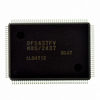
DF2437FV
Description
IC H8S/2437 MCU FLASH 128QFP
Manufacturer
Renesas Electronics America
Series
H8® H8S/2400r
Specifications of DF2437FV
Core Processor
H8S/2600
Core Size
16-Bit
Speed
20MHz
Connectivity
I²C, SCI
Peripherals
POR, PWM, WDT
Number Of I /o
85
Program Memory Size
256KB (256K x 8)
Program Memory Type
FLASH
Ram Size
16K x 8
Voltage - Supply (vcc/vdd)
3 V ~ 3.6 V
Data Converters
A/D 16x10b
Oscillator Type
Internal
Operating Temperature
-20°C ~ 75°C
Package / Case
128-QFP
Lead Free Status / RoHS Status
Lead free / RoHS Compliant
Eeprom Size
-
Available stocks
Company
Part Number
Manufacturer
Quantity
Price
Company:

Part Number:
DF2437FV
Manufacturer:
Renesas Electronics America
Quantity:
10 000


Rev.2.00 May. 28, 2009 Page 10 of 732
REJ09B0059-0200
Type
Bus control
Interrupts
On-chip
emulator
8-bit PWM
timer (PWM)
Symbol
WAIT
RD
HWR
LWR
AS
CS3 to CS1
AH
NMI
IRQ7 to IRQ0 76 to 73
ExIRQ7 to
ExIRQ0
ETRST*
ETMS
ETDO
ETDI
ETCK
PW7 to PW0
ExPW7 to
ExPW0
2
Pin No.
22
18
19
14
20
91, 15, 17 Output Chip select signals for areas 3 to 1.
20
27
52 to 49
70 to 67
1 to 4
39
35
40
38
36
116, 117,
119, 124
97, 98,
48, 47,
76 to 73
I/O
Input
Output This pin is low when the external address space
Output This pin is low when the external address space
Output This pin is low when the external address space
Output This pin is low when address output on the
Output Address latch signal for address/data multiplex
Input
Input
Input
Input
Output
Input
Input
Output Pulse output pins for the PWM timer.
Name and Function
Requests insertion of a wait state in the bus
cycle when accessing an external 3-state
address space.
is being read.
is to be written to, and the upper half of the data
bus is enabled.
is to be written to, and the lower half of the data
bus is enabled.
address bus is valid.
bus.
Nonmaskable interrupt request input pin
These pins request a maskable interrupt.
Selectable to which pin of IRQn or ExIRQn to
input IRQ7 to IRQ0 interrupts.
Interface pins for the on-chip emulator.
Reset by holding the ETRST pin to low when
activating the H-UDI. At this time, the ETRST pin
should be held low for 20 clocks of ETCK. For
details, see section 24, Electrical
Characteristics. Then, to activate the H-UDI, the
ETRST pin should be set to 1 and desired
values should be set to the ETCK, ETMS, and
ETDI pins. When in the normal operation without
activating the H-UDI, the ETRST, ETCK, ETMS,
and ETDI pins should be set to 1 or high-
impedance. Since these pins are internally
pulled up, care should be taken in the standby
state.
Selectable from which pin of PWn or ExPWn to
output PW5 to PW0.
Related parts for DF2437FV
Image
Part Number
Description
Manufacturer
Datasheet
Request
R

Part Number:
Description:
KIT STARTER FOR M16C/29
Manufacturer:
Renesas Electronics America
Datasheet:

Part Number:
Description:
KIT STARTER FOR R8C/2D
Manufacturer:
Renesas Electronics America
Datasheet:

Part Number:
Description:
R0K33062P STARTER KIT
Manufacturer:
Renesas Electronics America
Datasheet:

Part Number:
Description:
KIT STARTER FOR R8C/23 E8A
Manufacturer:
Renesas Electronics America
Datasheet:

Part Number:
Description:
KIT STARTER FOR R8C/25
Manufacturer:
Renesas Electronics America
Datasheet:

Part Number:
Description:
KIT STARTER H8S2456 SHARPE DSPLY
Manufacturer:
Renesas Electronics America
Datasheet:

Part Number:
Description:
KIT STARTER FOR R8C38C
Manufacturer:
Renesas Electronics America
Datasheet:

Part Number:
Description:
KIT STARTER FOR R8C35C
Manufacturer:
Renesas Electronics America
Datasheet:

Part Number:
Description:
KIT STARTER FOR R8CL3AC+LCD APPS
Manufacturer:
Renesas Electronics America
Datasheet:
Part Number:
Description:
KIT STARTER FOR RX610
Manufacturer:
Renesas Electronics America
Datasheet:

Part Number:
Description:
KIT STARTER FOR R32C/118
Manufacturer:
Renesas Electronics America
Datasheet:

Part Number:
Description:
KIT DEV RSK-R8C/26-29
Manufacturer:
Renesas Electronics America
Datasheet:

Part Number:
Description:
KIT STARTER FOR SH7124
Manufacturer:
Renesas Electronics America
Datasheet:

Part Number:
Description:
KIT STARTER FOR H8SX/1622
Manufacturer:
Renesas Electronics America
Datasheet:

Part Number:
Description:
KIT DEV FOR SH7203
Manufacturer:
Renesas Electronics America
Datasheet: