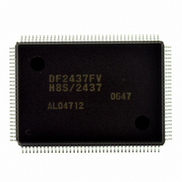
DF2437FV Renesas Electronics America, DF2437FV Datasheet - Page 622

DF2437FV
Manufacturer Part Number
DF2437FV
Description
IC H8S/2437 MCU FLASH 128QFP
Manufacturer
Renesas Electronics America
Series
H8® H8S/2400r
Specifications of DF2437FV
Core Processor
H8S/2600
Core Size
16-Bit
Speed
20MHz
Connectivity
I²C, SCI
Peripherals
POR, PWM, WDT
Number Of I /o
85
Program Memory Size
256KB (256K x 8)
Program Memory Type
FLASH
Ram Size
16K x 8
Voltage - Supply (vcc/vdd)
3 V ~ 3.6 V
Data Converters
A/D 16x10b
Oscillator Type
Internal
Operating Temperature
-20°C ~ 75°C
Package / Case
128-QFP
Lead Free Status / RoHS Status
Lead free / RoHS Compliant
Eeprom Size
-
Available stocks
Company
Part Number
Manufacturer
Quantity
Price
Company:
Part Number:
DF2437FV
Manufacturer:
Renesas Electronics America
Quantity:
10 000
- Current page: 622 of 776
- Download datasheet (5Mb)
128-byte programming is performed in one program processing. When more than 128-byte
programming is performed, programming destination address/program data parameter is updated
in 128-byte units and programming is repeated.
When less than 128-byte programming is performed, data size must be128 bytes by adding the
invalid data. If the invalid data to be added is set to H'FF, the program processing period can be
shortened.
1. Select the on-chip program to be downloaded and specify a download destination
2. Write H'A5 to FKEY
3. Set 1 to the SCO bit in FCCS and then execute downloading
• The user-MAT space is switched to the on-chip program storage area.
• After the selection condition of the download program and the FTDAR setting are checked, the
• FPCS, FECS, and the SCO bit in FCCS are cleared to 0.
• The return value is set to DPFR.
• After the on-chip program storage area is returned to the user-MAT space, the user procedure
• In download processing, the values of general registers of the CPU are retained.
Rev.2.00 May. 28, 2009 Page 582 of 732
REJ09B0059-0200
When the PPVS bit in FPCS is set to 1, the programming program is selected. Several
programming/erasing programs cannot be selected at one time. If several programs are set,
download is not performed and a download error is returned to the SS bit in DPFR. The start
address of a download destination is specified by FTDAR.
If H'A5 is not written to FKEY for protection, 1 cannot be set to the SCO bit for a download
request.
To set 1 to the SCO bit, the following conditions must be satisfied.
A H'A5 is written to FKEY.
B The SCO bit writing is executed in the on-chip RAM.
When the SCO bit is set to 1, download is started automatically. When the user procedure
program is returned, the SCO bit is cleared to 0. Therefore, the SCO bit cannot be confirmed to
be 1 in the user procedure program.
The download result can be confirmed only by the return value of DPFR. Before the SCO bit is
set to 1, incorrect determination must be prevented by setting the one byte of the start address
specified by FTDAR (to be used as DPFR) to a value other than the return value (H'FF).
When download is executed, particular interrupt processing, which is accompanied by the bank
switch as described below, is performed as internal microcomputer processing. Four NOP
instructions should be executed immediately after an instruction that sets the SCO bit to 1.
transfer processing to the on-chip RAM specified by FTDAR is executed.
program is returned.
Related parts for DF2437FV
Image
Part Number
Description
Manufacturer
Datasheet
Request
R

Part Number:
Description:
KIT STARTER FOR M16C/29
Manufacturer:
Renesas Electronics America
Datasheet:

Part Number:
Description:
KIT STARTER FOR R8C/2D
Manufacturer:
Renesas Electronics America
Datasheet:

Part Number:
Description:
R0K33062P STARTER KIT
Manufacturer:
Renesas Electronics America
Datasheet:

Part Number:
Description:
KIT STARTER FOR R8C/23 E8A
Manufacturer:
Renesas Electronics America
Datasheet:

Part Number:
Description:
KIT STARTER FOR R8C/25
Manufacturer:
Renesas Electronics America
Datasheet:

Part Number:
Description:
KIT STARTER H8S2456 SHARPE DSPLY
Manufacturer:
Renesas Electronics America
Datasheet:

Part Number:
Description:
KIT STARTER FOR R8C38C
Manufacturer:
Renesas Electronics America
Datasheet:

Part Number:
Description:
KIT STARTER FOR R8C35C
Manufacturer:
Renesas Electronics America
Datasheet:

Part Number:
Description:
KIT STARTER FOR R8CL3AC+LCD APPS
Manufacturer:
Renesas Electronics America
Datasheet:

Part Number:
Description:
KIT STARTER FOR RX610
Manufacturer:
Renesas Electronics America
Datasheet:

Part Number:
Description:
KIT STARTER FOR R32C/118
Manufacturer:
Renesas Electronics America
Datasheet:

Part Number:
Description:
KIT DEV RSK-R8C/26-29
Manufacturer:
Renesas Electronics America
Datasheet:

Part Number:
Description:
KIT STARTER FOR SH7124
Manufacturer:
Renesas Electronics America
Datasheet:

Part Number:
Description:
KIT STARTER FOR H8SX/1622
Manufacturer:
Renesas Electronics America
Datasheet:

Part Number:
Description:
KIT DEV FOR SH7203
Manufacturer:
Renesas Electronics America
Datasheet:


