DF2437FV Renesas Electronics America, DF2437FV Datasheet - Page 22
DF2437FV
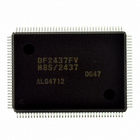
Manufacturer Part Number
DF2437FV
Description
IC H8S/2437 MCU FLASH 128QFP
Manufacturer
Renesas Electronics America
Series
H8® H8S/2400r
Specifications of DF2437FV
Core Processor
H8S/2600
Core Size
16-Bit
Speed
20MHz
Connectivity
I²C, SCI
Peripherals
POR, PWM, WDT
Number Of I /o
85
Program Memory Size
256KB (256K x 8)
Program Memory Type
FLASH
Ram Size
16K x 8
Voltage - Supply (vcc/vdd)
3 V ~ 3.6 V
Data Converters
A/D 16x10b
Oscillator Type
Internal
Operating Temperature
-20°C ~ 75°C
Package / Case
128-QFP
Lead Free Status / RoHS Status
Lead free / RoHS Compliant
Eeprom Size
-
Available stocks
Company
Part Number
Manufacturer
Quantity
Price
Company:

Part Number:
DF2437FV
Manufacturer:
Renesas Electronics America
Quantity:
10 000


18.5 Interrupt Source ................................................................................................................ 542
18.6 A/D Conversion Accuracy Definitions ............................................................................. 542
18.7 Usage Notes ...................................................................................................................... 544
Section 19 RAM ................................................................................................547
Section 20 Flash Memory (0.18-μm F-ZTAT Version)....................................549
20.1 Features............................................................................................................................. 549
20.2 Input/Output Pins .............................................................................................................. 557
20.3 Register Descriptions ........................................................................................................ 557
20.4 On-Board Programming Mode ......................................................................................... 575
20.5 Protection .......................................................................................................................... 603
20.6 Switching between User MAT and User Boot MAT ........................................................ 605
20.7 Programmer Mode ............................................................................................................ 607
20.8 Serial Communication Interface Specification for Boot Mode......................................... 608
20.9 Usage Notes ...................................................................................................................... 634
Section 21 Clock Pulse Generator .....................................................................637
21.1 Register Description.......................................................................................................... 638
21.2 Oscillator........................................................................................................................... 640
Rev.2.00 May. 28, 2009 Page xx of xxxviii
REJ09B0059-0200
18.4.4 External Trigger Input Timing............................................................................. 541
18.7.1 Module Stop Mode Setting .................................................................................. 544
18.7.2 Permissible Signal Source Impedance ................................................................. 544
18.7.3 Influences on Absolute Accuracy ........................................................................ 545
18.7.4 Setting Range of Analog Power Supply and Other Pins ...................................... 545
18.7.5 Notes on Board Design ........................................................................................ 545
18.7.6 Notes on Noise Countermeasures ........................................................................ 545
20.1.1 Mode Transition................................................................................................... 551
20.1.2 Mode Comparison................................................................................................ 552
20.1.3 Flash Memory MAT Configuration ..................................................................... 553
20.1.4 Block Division ..................................................................................................... 554
20.1.5 Programming/Erasing Interface ........................................................................... 555
20.3.1 Programming/Erasing Interface Registers ........................................................... 558
20.3.2 Programming/Erasing Interface Parameters ........................................................ 565
20.4.1 Boot Mode ........................................................................................................... 575
20.4.2 User Program Mode............................................................................................. 579
20.4.3 User Boot Mode................................................................................................... 589
20.4.4 Storable Area for Procedure Program and Program Data .................................... 593
20.5.1 Hardware Protection ............................................................................................ 603
20.5.2 Software Protection.............................................................................................. 604
20.5.3 Error Protection.................................................................................................... 604
21.1.1 System Clock Control Register (SCKCR) ........................................................... 638
Related parts for DF2437FV
Image
Part Number
Description
Manufacturer
Datasheet
Request
R

Part Number:
Description:
KIT STARTER FOR M16C/29
Manufacturer:
Renesas Electronics America
Datasheet:

Part Number:
Description:
KIT STARTER FOR R8C/2D
Manufacturer:
Renesas Electronics America
Datasheet:

Part Number:
Description:
R0K33062P STARTER KIT
Manufacturer:
Renesas Electronics America
Datasheet:

Part Number:
Description:
KIT STARTER FOR R8C/23 E8A
Manufacturer:
Renesas Electronics America
Datasheet:

Part Number:
Description:
KIT STARTER FOR R8C/25
Manufacturer:
Renesas Electronics America
Datasheet:

Part Number:
Description:
KIT STARTER H8S2456 SHARPE DSPLY
Manufacturer:
Renesas Electronics America
Datasheet:

Part Number:
Description:
KIT STARTER FOR R8C38C
Manufacturer:
Renesas Electronics America
Datasheet:

Part Number:
Description:
KIT STARTER FOR R8C35C
Manufacturer:
Renesas Electronics America
Datasheet:

Part Number:
Description:
KIT STARTER FOR R8CL3AC+LCD APPS
Manufacturer:
Renesas Electronics America
Datasheet:
Part Number:
Description:
KIT STARTER FOR RX610
Manufacturer:
Renesas Electronics America
Datasheet:

Part Number:
Description:
KIT STARTER FOR R32C/118
Manufacturer:
Renesas Electronics America
Datasheet:

Part Number:
Description:
KIT DEV RSK-R8C/26-29
Manufacturer:
Renesas Electronics America
Datasheet:

Part Number:
Description:
KIT STARTER FOR SH7124
Manufacturer:
Renesas Electronics America
Datasheet:

Part Number:
Description:
KIT STARTER FOR H8SX/1622
Manufacturer:
Renesas Electronics America
Datasheet:

Part Number:
Description:
KIT DEV FOR SH7203
Manufacturer:
Renesas Electronics America
Datasheet: