DF2437FV Renesas Electronics America, DF2437FV Datasheet - Page 37
DF2437FV
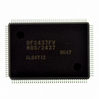
Manufacturer Part Number
DF2437FV
Description
IC H8S/2437 MCU FLASH 128QFP
Manufacturer
Renesas Electronics America
Series
H8® H8S/2400r
Specifications of DF2437FV
Core Processor
H8S/2600
Core Size
16-Bit
Speed
20MHz
Connectivity
I²C, SCI
Peripherals
POR, PWM, WDT
Number Of I /o
85
Program Memory Size
256KB (256K x 8)
Program Memory Type
FLASH
Ram Size
16K x 8
Voltage - Supply (vcc/vdd)
3 V ~ 3.6 V
Data Converters
A/D 16x10b
Oscillator Type
Internal
Operating Temperature
-20°C ~ 75°C
Package / Case
128-QFP
Lead Free Status / RoHS Status
Lead free / RoHS Compliant
Eeprom Size
-
Available stocks
Company
Part Number
Manufacturer
Quantity
Price
Company:

Part Number:
DF2437FV
Manufacturer:
Renesas Electronics America
Quantity:
10 000


Table 11.4
Table 11.5
Section 12 16-Bit Timer Pulse Unit (TPU)
Table 12.1
Table 12.2
Table 12.3
Table 12.4
Table 12.5
Table 12.6
Table 12.7
Table 12.8
Table 12.9
Table 12.10
Table 12.11
Table 12.12
Table 12.13
Table 12.14
Table 12.15
Table 12.16
Table 12.17
Table 12.18
Table 12.19
Table 12.20
Table 12.21
Table 12.22
Table 12.23
Table 12.24
Table 12.25
Section 13 Timer Connection
Table 13.1
Table 13.2
Table 13.3
Table 13.4
Table 13.5
Table 13.6
Table 13.7
Table 13.8
Table 13.9
Table 13.10
Table 13.11
Timer Output Priorities ........................................................................................306
Switching of Internal Clocks and TCNT Operation.............................................307
TPU Functions .....................................................................................................311
Pin Configuration.................................................................................................313
CCLR2 to CCLR0 (Channel 0)............................................................................316
CCLR2 to CCLR0 (Channels 1 and 2) ................................................................316
TPSC2 to TPSC0 (Channel 0) .............................................................................317
TPSC2 to TPSC0 (Channel 1) .............................................................................317
TPSC2 to TPSC0 (Channel 2) .............................................................................318
MD3 to MD0........................................................................................................319
TIORH_0 (Channel 0) .........................................................................................321
TIORH_0 (Channel 0) .........................................................................................322
TIORL_0 (Channel 0)..........................................................................................323
TIORL_0 (Channel 0)..........................................................................................324
TIOR_1 (Channel 1) ............................................................................................325
TIOR_1 (Channel 1) ............................................................................................326
TIOR_2 (Channel 2) ............................................................................................327
TIOR_2 (Channel 2) ............................................................................................328
Register Combinations in Buffer Operation.........................................................346
Cascaded Combinations.......................................................................................349
PWM Output Registers and Output Pins .............................................................352
Clock Input Pins for Phase Counting Mode.........................................................356
Up/Down-Count Conditions in Phase Counting Mode 1.....................................357
Up/Down-Count Conditions in Phase Counting Mode 2.....................................358
Up/Down-Count Conditions in Phase Counting Mode 3.....................................359
Up/Down-Count Conditions in Phase Counting Mode 4.....................................360
TPU Interrupts .....................................................................................................361
Pin Configuration.................................................................................................384
Synchronization Signal Connection Enable.........................................................387
HSYNCO Output Selection .................................................................................390
VSYNCO Output Selection .................................................................................390
Examples of TCR Settings...................................................................................397
Examples of TCORB (Pulse Width Threshold) Settings .....................................398
Examples of TCR and TCSR Settings .................................................................403
Examples of TCR, TCSR, TCOR, and OCRDM Settings ...................................405
Examples of TCR, TCSR, and TCORB Settings .................................................408
Examples of OCRAR, OCRAF, TOCR, TCORA, TCORB, TCR, and TCSR
HSYNCO Output Modes .....................................................................................414
Settings ................................................................................................................412
Rev.2.00 May. 28, 2009 Page xxxv of xxxviii
REJ09B0059-0200
Related parts for DF2437FV
Image
Part Number
Description
Manufacturer
Datasheet
Request
R

Part Number:
Description:
KIT STARTER FOR M16C/29
Manufacturer:
Renesas Electronics America
Datasheet:

Part Number:
Description:
KIT STARTER FOR R8C/2D
Manufacturer:
Renesas Electronics America
Datasheet:

Part Number:
Description:
R0K33062P STARTER KIT
Manufacturer:
Renesas Electronics America
Datasheet:

Part Number:
Description:
KIT STARTER FOR R8C/23 E8A
Manufacturer:
Renesas Electronics America
Datasheet:

Part Number:
Description:
KIT STARTER FOR R8C/25
Manufacturer:
Renesas Electronics America
Datasheet:

Part Number:
Description:
KIT STARTER H8S2456 SHARPE DSPLY
Manufacturer:
Renesas Electronics America
Datasheet:

Part Number:
Description:
KIT STARTER FOR R8C38C
Manufacturer:
Renesas Electronics America
Datasheet:

Part Number:
Description:
KIT STARTER FOR R8C35C
Manufacturer:
Renesas Electronics America
Datasheet:

Part Number:
Description:
KIT STARTER FOR R8CL3AC+LCD APPS
Manufacturer:
Renesas Electronics America
Datasheet:
Part Number:
Description:
KIT STARTER FOR RX610
Manufacturer:
Renesas Electronics America
Datasheet:

Part Number:
Description:
KIT STARTER FOR R32C/118
Manufacturer:
Renesas Electronics America
Datasheet:

Part Number:
Description:
KIT DEV RSK-R8C/26-29
Manufacturer:
Renesas Electronics America
Datasheet:

Part Number:
Description:
KIT STARTER FOR SH7124
Manufacturer:
Renesas Electronics America
Datasheet:

Part Number:
Description:
KIT STARTER FOR H8SX/1622
Manufacturer:
Renesas Electronics America
Datasheet:

Part Number:
Description:
KIT DEV FOR SH7203
Manufacturer:
Renesas Electronics America
Datasheet: