DF2437FV Renesas Electronics America, DF2437FV Datasheet - Page 29
DF2437FV
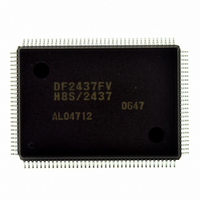
Manufacturer Part Number
DF2437FV
Description
IC H8S/2437 MCU FLASH 128QFP
Manufacturer
Renesas Electronics America
Series
H8® H8S/2400r
Specifications of DF2437FV
Core Processor
H8S/2600
Core Size
16-Bit
Speed
20MHz
Connectivity
I²C, SCI
Peripherals
POR, PWM, WDT
Number Of I /o
85
Program Memory Size
256KB (256K x 8)
Program Memory Type
FLASH
Ram Size
16K x 8
Voltage - Supply (vcc/vdd)
3 V ~ 3.6 V
Data Converters
A/D 16x10b
Oscillator Type
Internal
Operating Temperature
-20°C ~ 75°C
Package / Case
128-QFP
Lead Free Status / RoHS Status
Lead free / RoHS Compliant
Eeprom Size
-
Available stocks
Company
Part Number
Manufacturer
Quantity
Price
Company:

Part Number:
DF2437FV
Manufacturer:
Renesas Electronics America
Quantity:
10 000


Figure 12.39 Buffer Operation Timing (Compare Match) ........................................................366
Figure 12.40 Buffer Operation Timing (Input Capture)............................................................366
Figure 12.41 TGI Interrupt Timing (Compare Match)..............................................................367
Figure 12.42 TGI Interrupt Timing (Input Capture)..................................................................368
Figure 12.43 TCIV Interrupt Setting Timing ............................................................................369
Figure 12.44 TCIU Interrupt Setting Timing ............................................................................369
Figure 12.45 Timing for Status Flag Clearing by CPU .............................................................370
Figure 12.46 Phase Difference, Overlap, and Pulse Width in Phase Counting Mode...............371
Figure 12.47 Contention between TCNT Write and Clear Operations .....................................372
Figure 12.48 Contention between TCNT Write and Increment Operations..............................372
Figure 12.49 Contention between TGR Write and Compare Match .........................................373
Figure 12.50 Contention between Buffer Register Write and Compare Match ........................374
Figure 12.51 Contention between TGR Read and Input Capture..............................................375
Figure 12.52 Contention between TGR Write and Input Capture.............................................376
Figure 12.53 Contention between Buffer Register Write and Input Capture ............................377
Figure 12.54 Contention between Overflow and Counter Clearing ..........................................378
Figure 12.55 Contention between TCNT Write and Overflow .................................................378
Section 13 Timer Connection
Figure 13.1
Figure 13.2
Figure 13.3
Figure 13.4
Figure 13.5
Figure 13.6
Figure 13.7
Figure 13.8
Figure 13.9
Figure 13.10 Block Diagram for 2fH Modification of IHI Signal.............................................405
Figure 13.11 2fH Modification Timing Chart ...........................................................................406
Figure 13.12 Block Diagram for IVI Signal Fall Modification and IHI Signal Operation........407
Figure 13.13 Fall Modification and IHI Synchronization Timing Chart...................................408
Figure 13.14 Block Diagram for IVG Signal Generation..........................................................410
Figure 13.15 Block Diagram for IHG Signal Generation..........................................................411
Figure 13.16 IVG Signal/IHG Signal/CL4 Signal Timing Chart ..............................................413
Figure 13.17 CBLANK Output Waveform Generation ............................................................416
Section 14 Duty Measurement Circuit
Figure 14.1
Figure 14.2
Figure 14.3
Figure 14.4
Schematic Diagram of Timer Connection............................................................382
Block Diagram of Timer Connection...................................................................383
Block Diagram for PWM Decoding ....................................................................397
Timing Chart for PWM Decoding .......................................................................398
Block Diagram for Clamp Waveform Generation ...............................................400
Timing Chart for Clamp Waveform Generation (CL1 and CL2 Signals) ............401
Timing Chart for Clamp Waveform Generation (CL3 Signal) ............................401
Block Diagram for Measurement of 8-Bit Timer Divided Waveform Period......402
Timing Chart for Measurement of IVI Signal and
Block Diagram of Duty Measurement Circuit .....................................................418
Example of Duty Measurement for External Event Signal..................................424
TWCNT Count Timing........................................................................................425
TWCNT Clear Timing by Setting START Bit ....................................................425
IHI Signal Divided Waveform Periods ................................................................404
Rev.2.00 May. 28, 2009 Page xxvii of xxxviii
REJ09B0059-0200
Related parts for DF2437FV
Image
Part Number
Description
Manufacturer
Datasheet
Request
R

Part Number:
Description:
KIT STARTER FOR M16C/29
Manufacturer:
Renesas Electronics America
Datasheet:

Part Number:
Description:
KIT STARTER FOR R8C/2D
Manufacturer:
Renesas Electronics America
Datasheet:

Part Number:
Description:
R0K33062P STARTER KIT
Manufacturer:
Renesas Electronics America
Datasheet:

Part Number:
Description:
KIT STARTER FOR R8C/23 E8A
Manufacturer:
Renesas Electronics America
Datasheet:

Part Number:
Description:
KIT STARTER FOR R8C/25
Manufacturer:
Renesas Electronics America
Datasheet:

Part Number:
Description:
KIT STARTER H8S2456 SHARPE DSPLY
Manufacturer:
Renesas Electronics America
Datasheet:

Part Number:
Description:
KIT STARTER FOR R8C38C
Manufacturer:
Renesas Electronics America
Datasheet:

Part Number:
Description:
KIT STARTER FOR R8C35C
Manufacturer:
Renesas Electronics America
Datasheet:

Part Number:
Description:
KIT STARTER FOR R8CL3AC+LCD APPS
Manufacturer:
Renesas Electronics America
Datasheet:
Part Number:
Description:
KIT STARTER FOR RX610
Manufacturer:
Renesas Electronics America
Datasheet:

Part Number:
Description:
KIT STARTER FOR R32C/118
Manufacturer:
Renesas Electronics America
Datasheet:

Part Number:
Description:
KIT DEV RSK-R8C/26-29
Manufacturer:
Renesas Electronics America
Datasheet:

Part Number:
Description:
KIT STARTER FOR SH7124
Manufacturer:
Renesas Electronics America
Datasheet:

Part Number:
Description:
KIT STARTER FOR H8SX/1622
Manufacturer:
Renesas Electronics America
Datasheet:

Part Number:
Description:
KIT DEV FOR SH7203
Manufacturer:
Renesas Electronics America
Datasheet: