D12321VF25V Renesas Electronics America, D12321VF25V Datasheet - Page 464
D12321VF25V
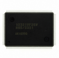
Manufacturer Part Number
D12321VF25V
Description
IC H8S/2300 MCU ROMLESS 128QFP
Manufacturer
Renesas Electronics America
Series
H8® H8S/2300r
Datasheets
1.HEWH8E10A.pdf
(19 pages)
2.D12312SVTE25V.pdf
(341 pages)
3.D12322RVF25V.pdf
(1304 pages)
Specifications of D12321VF25V
Core Processor
H8S/2000
Core Size
16-Bit
Speed
25MHz
Connectivity
SCI, SmartCard
Peripherals
POR, PWM, WDT
Number Of I /o
86
Program Memory Type
ROMless
Ram Size
4K x 8
Voltage - Supply (vcc/vdd)
2.7 V ~ 3.6 V
Data Converters
A/D 8x10b; D/A 2x8b
Oscillator Type
Internal
Operating Temperature
-20°C ~ 75°C
Package / Case
128-QFP
For Use With
EDK2329 - DEV EVALUATION KIT H8S/2329
Lead Free Status / RoHS Status
Lead free / RoHS Compliant
Eeprom Size
-
Program Memory Size
-
Available stocks
Company
Part Number
Manufacturer
Quantity
Price
Company:

Part Number:
D12321VF25V
Manufacturer:
Renesas Electronics America
Quantity:
135
Company:
Part Number:
D12321VF25V
Manufacturer:
Renesas
Quantity:
675
Company:
Part Number:
D12321VF25V
Manufacturer:
Renesas Electronics America
Quantity:
10 000


Section 9 I/O Ports
Bits 2 to 0—Reserved: These bits are always read as 0.
System Control Register (SYSCR)
SYSCR is an 8-bit readable/writable register that selects the interrupt control mode, controls the
LWR pin, switches the IRQ
initialized to H'01 by a reset, and in hardware standby mode. It is not initialized in software
standby mode.
Bits 5 and 4—Interrupt Control Mode 1 and 0 (INTM1, INTM0): These bits select either of
two interrupt control modes for the interrupt controller. For details, see section 5, Interrupt
Controller.
Bit 3—NMI Edge Select (NMIEG): Selects the input edge for the NMI pin. For details, see
section 5, Interrupt Controller.
Bit 2—LWR Output Disable (LWROD): Enables or disables LWR output. This bit is valid in
modes 4 to 6.
Bit 2
LWROD
0
1
Bit 1—IRQ Port Switching Select (IRQPAS): Selects switching of input pins for IRQ
For details, see section 9.6, Port 5.
Bit 0—RAM Enable (RAME): Enables or disables on-chip RAM. For details, see section 18,
RAM.
Rev.6.00 Sep. 27, 2007 Page 432 of 1268
REJ09B0220-0600
Bit
Initial value :
R/W
:
:
PF
PF
Description
R/W
—
7
0
3
3
is designated as LWR output pin
is designated as I/O port, and does not function as LWR output pin
4
to IRQ
—
—
6
0
7
input pins, and selects the detected edge for NMI. SYSCR is
INTM1
R/W
5
0
INTM0
R/W
4
0
NMIEG
R/W
3
0
LWROE IRQPAS
R/W
2
0
R/W
1
0
(Initial value)
4
to IRQ
RAME
R/W
0
1
7
.
Related parts for D12321VF25V
Image
Part Number
Description
Manufacturer
Datasheet
Request
R

Part Number:
Description:
KIT STARTER FOR M16C/29
Manufacturer:
Renesas Electronics America
Datasheet:

Part Number:
Description:
KIT STARTER FOR R8C/2D
Manufacturer:
Renesas Electronics America
Datasheet:

Part Number:
Description:
R0K33062P STARTER KIT
Manufacturer:
Renesas Electronics America
Datasheet:

Part Number:
Description:
KIT STARTER FOR R8C/23 E8A
Manufacturer:
Renesas Electronics America
Datasheet:

Part Number:
Description:
KIT STARTER FOR R8C/25
Manufacturer:
Renesas Electronics America
Datasheet:

Part Number:
Description:
KIT STARTER H8S2456 SHARPE DSPLY
Manufacturer:
Renesas Electronics America
Datasheet:

Part Number:
Description:
KIT STARTER FOR R8C38C
Manufacturer:
Renesas Electronics America
Datasheet:

Part Number:
Description:
KIT STARTER FOR R8C35C
Manufacturer:
Renesas Electronics America
Datasheet:

Part Number:
Description:
KIT STARTER FOR R8CL3AC+LCD APPS
Manufacturer:
Renesas Electronics America
Datasheet:
Part Number:
Description:
KIT STARTER FOR RX610
Manufacturer:
Renesas Electronics America
Datasheet:

Part Number:
Description:
KIT STARTER FOR R32C/118
Manufacturer:
Renesas Electronics America
Datasheet:

Part Number:
Description:
KIT DEV RSK-R8C/26-29
Manufacturer:
Renesas Electronics America
Datasheet:

Part Number:
Description:
KIT STARTER FOR SH7124
Manufacturer:
Renesas Electronics America
Datasheet:

Part Number:
Description:
KIT STARTER FOR H8SX/1622
Manufacturer:
Renesas Electronics America
Datasheet:

Part Number:
Description:
KIT DEV FOR SH7203
Manufacturer:
Renesas Electronics America
Datasheet: