D12321VF25V Renesas Electronics America, D12321VF25V Datasheet - Page 641
D12321VF25V
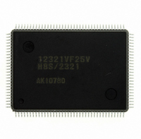
Manufacturer Part Number
D12321VF25V
Description
IC H8S/2300 MCU ROMLESS 128QFP
Manufacturer
Renesas Electronics America
Series
H8® H8S/2300r
Datasheets
1.HEWH8E10A.pdf
(19 pages)
2.D12312SVTE25V.pdf
(341 pages)
3.D12322RVF25V.pdf
(1304 pages)
Specifications of D12321VF25V
Core Processor
H8S/2000
Core Size
16-Bit
Speed
25MHz
Connectivity
SCI, SmartCard
Peripherals
POR, PWM, WDT
Number Of I /o
86
Program Memory Type
ROMless
Ram Size
4K x 8
Voltage - Supply (vcc/vdd)
2.7 V ~ 3.6 V
Data Converters
A/D 8x10b; D/A 2x8b
Oscillator Type
Internal
Operating Temperature
-20°C ~ 75°C
Package / Case
128-QFP
For Use With
EDK2329 - DEV EVALUATION KIT H8S/2329
Lead Free Status / RoHS Status
Lead free / RoHS Compliant
Eeprom Size
-
Program Memory Size
-
Available stocks
Company
Part Number
Manufacturer
Quantity
Price
Company:

Part Number:
D12321VF25V
Manufacturer:
Renesas Electronics America
Quantity:
135
Company:
Part Number:
D12321VF25V
Manufacturer:
Renesas
Quantity:
675
Company:
Part Number:
D12321VF25V
Manufacturer:
Renesas Electronics America
Quantity:
10 000


Bit 3—Multiprocessor Interrupt Enable (MPIE): Enables or disables multiprocessor interrupts.
The MPIE bit setting is only valid in asynchronous mode when the MP bit in SMR is set to 1.
The MPIE bit setting is invalid in synchronous mode or when the MP bit is cleared to 0.
Bit 3
MPIE
0
1
Note: * When receive data including MPB = 0 is received, receive data transfer from RSR to RDR,
Bit 2—Transmit End Interrupt Enable (TEIE): Enables or disables transmit-end interrupt
(TEI) request generation when there is no valid transmit data in TDR in MSB data transmission.
Bit 2
TEIE
0
1
Note: * TEI cancellation can be performed by reading 1 from the TDRE flag in SSR, then clearing it
Bits 1 and 0—Clock Enable 1 and 0 (CKE1, CKE0): These bits are used to select the SCI clock
source and enable or disable clock output from the SCK pin. The combination of the CKE1 and
CKE0 bits determines whether the SCK pin functions as an I/O port, the serial clock output pin, or
the serial clock input pin.
The setting of the CKE0 bit, however, is only valid for internal clock operation (CKE1 = 0) in
asynchronous mode. The CKE0 bit setting is invalid in synchronous mode, and in the case of
external clock operation (CKE1 = 1). Set CKE1 and CKE0 before determining the SCI operating
mode with SMR.
receive error detection, and setting of the RDRF, FER, and ORER flags in SSR, is not
performed. When receive data including MPB = 1 is received, the MPB bit in SSR is set to
1, the MPIE bit is cleared to 0 automatically, and generation of RXI and ERI interrupts
(when the TIE and RIE bits in SCR are set to 1) and FER and ORER flag setting is enabled.
to 0 and clearing the TEND flag to 0, or by clearing the TEIE bit to 0.
Description
Multiprocessor interrupts disabled (normal reception performed)
[Clearing conditions]
•
•
Multiprocessor interrupts enabled *
Receive-data-full interrupt (RXI) requests, receive-error interrupt (ERI) requests, and
setting of the RDRF, FER, and ORER flags in SSR are disabled until data with the
multiprocessor bit set to 1 is received.
Description
Transmit end interrupt (TEI) request disabled *
Transmit end interrupt (TEI) request enabled *
When the MPIE bit is cleared to 0
When data with MPB = 1 is received
Section 14 Serial Communication Interface (SCI)
Rev.6.00 Sep. 27, 2007 Page 609 of 1268
REJ09B0220-0600
(Initial value)
(Initial value)
Related parts for D12321VF25V
Image
Part Number
Description
Manufacturer
Datasheet
Request
R

Part Number:
Description:
KIT STARTER FOR M16C/29
Manufacturer:
Renesas Electronics America
Datasheet:

Part Number:
Description:
KIT STARTER FOR R8C/2D
Manufacturer:
Renesas Electronics America
Datasheet:

Part Number:
Description:
R0K33062P STARTER KIT
Manufacturer:
Renesas Electronics America
Datasheet:

Part Number:
Description:
KIT STARTER FOR R8C/23 E8A
Manufacturer:
Renesas Electronics America
Datasheet:

Part Number:
Description:
KIT STARTER FOR R8C/25
Manufacturer:
Renesas Electronics America
Datasheet:

Part Number:
Description:
KIT STARTER H8S2456 SHARPE DSPLY
Manufacturer:
Renesas Electronics America
Datasheet:

Part Number:
Description:
KIT STARTER FOR R8C38C
Manufacturer:
Renesas Electronics America
Datasheet:

Part Number:
Description:
KIT STARTER FOR R8C35C
Manufacturer:
Renesas Electronics America
Datasheet:

Part Number:
Description:
KIT STARTER FOR R8CL3AC+LCD APPS
Manufacturer:
Renesas Electronics America
Datasheet:
Part Number:
Description:
KIT STARTER FOR RX610
Manufacturer:
Renesas Electronics America
Datasheet:

Part Number:
Description:
KIT STARTER FOR R32C/118
Manufacturer:
Renesas Electronics America
Datasheet:

Part Number:
Description:
KIT DEV RSK-R8C/26-29
Manufacturer:
Renesas Electronics America
Datasheet:

Part Number:
Description:
KIT STARTER FOR SH7124
Manufacturer:
Renesas Electronics America
Datasheet:

Part Number:
Description:
KIT STARTER FOR H8SX/1622
Manufacturer:
Renesas Electronics America
Datasheet:

Part Number:
Description:
KIT DEV FOR SH7203
Manufacturer:
Renesas Electronics America
Datasheet: