D12321VF25V Renesas Electronics America, D12321VF25V Datasheet - Page 912
D12321VF25V
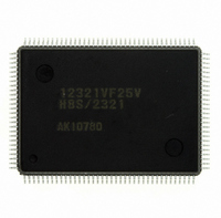
Manufacturer Part Number
D12321VF25V
Description
IC H8S/2300 MCU ROMLESS 128QFP
Manufacturer
Renesas Electronics America
Series
H8® H8S/2300r
Datasheets
1.HEWH8E10A.pdf
(19 pages)
2.D12312SVTE25V.pdf
(341 pages)
3.D12322RVF25V.pdf
(1304 pages)
Specifications of D12321VF25V
Core Processor
H8S/2000
Core Size
16-Bit
Speed
25MHz
Connectivity
SCI, SmartCard
Peripherals
POR, PWM, WDT
Number Of I /o
86
Program Memory Type
ROMless
Ram Size
4K x 8
Voltage - Supply (vcc/vdd)
2.7 V ~ 3.6 V
Data Converters
A/D 8x10b; D/A 2x8b
Oscillator Type
Internal
Operating Temperature
-20°C ~ 75°C
Package / Case
128-QFP
For Use With
EDK2329 - DEV EVALUATION KIT H8S/2329
Lead Free Status / RoHS Status
Lead free / RoHS Compliant
Eeprom Size
-
Program Memory Size
-
Available stocks
Company
Part Number
Manufacturer
Quantity
Price
Company:

Part Number:
D12321VF25V
Manufacturer:
Renesas Electronics America
Quantity:
135
Company:
Part Number:
D12321VF25V
Manufacturer:
Renesas
Quantity:
675
Company:
Part Number:
D12321VF25V
Manufacturer:
Renesas Electronics America
Quantity:
10 000


Section 19 ROM
Rev.6.00 Sep. 27, 2007 Page 880 of 1268
REJ09B0220-0600
Notes: 1. Data transfer is performed by byte transfer. The lower 8 bits of the first
Note 7: Write Pulse Width
Note: Use a (z3) µs write pulse for additional
5. A write pulse of (z1) or (z2) μs should be applied according to the progress
6. For the values of x, y, z1, z2, z3, α, β, γ, ε, η, θ, and N, see section 22.2.6, Flash Memory Characteristics.
2. Verify data is read in 16-bit (W) units.
3. Even bits for which programming has been completed in the 128-byte
4. A 128-byte area for storing program data, a 128-byte area for storing
Program Data Operation Chart
Number of Writes (n)
Original Data
Additional program data
Clear PSU1 (2) bit in FLMCR1 (2)
Write pulse application subroutine
Set PSU1 (2) bit in FLMCR1 (2)
Reprogram data area
Wait (z1) μs or (z2) μs or (z3) μs
of programming. See Note 7 for the pulse widths. When the additional program
data is programmed, a write pulse of (z3) μs should be applied. Reprogram data X' stands for reprogram data to which a write pulse has been applied.
address written to must be H'00 or H'80. A 128-byte data transfer must
be performed even if writing fewer than 128 bytes; in this case, H'FF
data must be written to the extra addresses.
programming loop will be subjected to additional programming if they
fail the subsequent verify operation.
reprogram data, and a 128-byte area for storing additional program data
should be provided in RAM. The contents of the reprogram data and
additional program data areas are modified as programming proceeds.
Program data area
Clear P1 (2) bit in FLMCR1 (2)
Set P1 (2) bit in FLMCR1 (2)
area (128 bytes)
(D)
programming.
0
1
Sub-routine write pulse
(128 bytes)
(128 bytes)
1000
998
999
10
11
12
13
1
2
3
4
5
6
7
8
9
.
.
.
RAM
Disable WDT
Enable WDT
Wait (α) μs
Wait (β) μs
Wait (y) μs
End sub
Verify Data
(V)
0
1
0
1
Write Time (z) μs
Reprogram Data
*6
Figure 19.71 Program/Program-Verify Flowchart
z1
z1
z1
z1
z1
z1
z2
z2
z2
z2
z2
z2
z2
z2
z2
z2
.
.
.
(X)
1
0
1
*6
*5 *6
*6
*6
Programming completed
Programming incomplete; reprogram
Still in erased state; no action
Increment address
Comments
Store 128-byte program data in program
NG
data area consecutively to flash memory
additional program data area in RAM to
Write 128-byte data in RAM reprogram
Transfer reprogram data to reprogram
Additional program data computation
H'FF dummy write to verify address
data area and reprogram data area
Transfer additional program data to
Sequentially write 128-byte data in
Clear SWE1 (2) bit in FLMCR1 (2)
Clear PV1 (2) bit in FLMCR1 (2)
Set SWE1 (2) bit in FLMCR1 (2)
Set PV1 (2) bit in FLMCR1 (2)
Reprogram data computation
additional program data area
(z3) µs additional write pulse
Start of programming
Additional Program Data Operation Chart
End of programming
Read data = verify
Reprogram
Read verify data
(z1) μs or (z2) μs
data verification
Data (X')
flash memory
Write Pulse
Wait (x) μs
Wait (γ) μs
Wait (ε) μs
completed?
Write pulse
Wait (η) μs
Wait (θ) μs
data area
128-byte
0
1
m = 0?
m = 0
6 ≥ n ?
6 ≥ n ?
data?
n = 1
Start
OK
OK
OK
OK
OK
Sub-routine-call
Verify Data
(V)
0
1
0
1
NG
NG
NG
NG
Program Data (Y)
Additional
*6
*6
*4
*1
See Note 7 for pulse width
*2
*3
*4
*1
*4
*6
*6
*6
*6
*6
Perform programming in the erased state.
Do not perform additional programming
on previously programmed addresses.
0
1
Clear SWE1 (2) bit in FLMCR1 (2)
m = 1
Programming failure
Additional programming executed
Additional programming not executed
Additional programming not executed
Additional programming not executed
Wait (θ) μs
n ≥ N?
OK
*6
Comments
NG
n ← n + 1
*6
Related parts for D12321VF25V
Image
Part Number
Description
Manufacturer
Datasheet
Request
R

Part Number:
Description:
KIT STARTER FOR M16C/29
Manufacturer:
Renesas Electronics America
Datasheet:

Part Number:
Description:
KIT STARTER FOR R8C/2D
Manufacturer:
Renesas Electronics America
Datasheet:

Part Number:
Description:
R0K33062P STARTER KIT
Manufacturer:
Renesas Electronics America
Datasheet:

Part Number:
Description:
KIT STARTER FOR R8C/23 E8A
Manufacturer:
Renesas Electronics America
Datasheet:

Part Number:
Description:
KIT STARTER FOR R8C/25
Manufacturer:
Renesas Electronics America
Datasheet:

Part Number:
Description:
KIT STARTER H8S2456 SHARPE DSPLY
Manufacturer:
Renesas Electronics America
Datasheet:

Part Number:
Description:
KIT STARTER FOR R8C38C
Manufacturer:
Renesas Electronics America
Datasheet:

Part Number:
Description:
KIT STARTER FOR R8C35C
Manufacturer:
Renesas Electronics America
Datasheet:

Part Number:
Description:
KIT STARTER FOR R8CL3AC+LCD APPS
Manufacturer:
Renesas Electronics America
Datasheet:
Part Number:
Description:
KIT STARTER FOR RX610
Manufacturer:
Renesas Electronics America
Datasheet:

Part Number:
Description:
KIT STARTER FOR R32C/118
Manufacturer:
Renesas Electronics America
Datasheet:

Part Number:
Description:
KIT DEV RSK-R8C/26-29
Manufacturer:
Renesas Electronics America
Datasheet:

Part Number:
Description:
KIT STARTER FOR SH7124
Manufacturer:
Renesas Electronics America
Datasheet:

Part Number:
Description:
KIT STARTER FOR H8SX/1622
Manufacturer:
Renesas Electronics America
Datasheet:

Part Number:
Description:
KIT DEV FOR SH7203
Manufacturer:
Renesas Electronics America
Datasheet: