D12321VF25V Renesas Electronics America, D12321VF25V Datasheet - Page 841
D12321VF25V
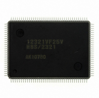
Manufacturer Part Number
D12321VF25V
Description
IC H8S/2300 MCU ROMLESS 128QFP
Manufacturer
Renesas Electronics America
Series
H8® H8S/2300r
Datasheets
1.HEWH8E10A.pdf
(19 pages)
2.D12312SVTE25V.pdf
(341 pages)
3.D12322RVF25V.pdf
(1304 pages)
Specifications of D12321VF25V
Core Processor
H8S/2000
Core Size
16-Bit
Speed
25MHz
Connectivity
SCI, SmartCard
Peripherals
POR, PWM, WDT
Number Of I /o
86
Program Memory Type
ROMless
Ram Size
4K x 8
Voltage - Supply (vcc/vdd)
2.7 V ~ 3.6 V
Data Converters
A/D 8x10b; D/A 2x8b
Oscillator Type
Internal
Operating Temperature
-20°C ~ 75°C
Package / Case
128-QFP
For Use With
EDK2329 - DEV EVALUATION KIT H8S/2329
Lead Free Status / RoHS Status
Lead free / RoHS Compliant
Eeprom Size
-
Program Memory Size
-
Available stocks
Company
Part Number
Manufacturer
Quantity
Price
Company:

Part Number:
D12321VF25V
Manufacturer:
Renesas Electronics America
Quantity:
135
Company:
Part Number:
D12321VF25V
Manufacturer:
Renesas
Quantity:
675
Company:
Part Number:
D12321VF25V
Manufacturer:
Renesas Electronics America
Quantity:
10 000


19.15
When pins are set to on-board programming mode, program/erase/verify operations can be
performed on the on-chip flash memory. There are two on-board programming modes: boot mode
and user program mode. The pin settings for transition to each of these modes are shown in table
19.30. For a diagram of the transitions to the various flash memory modes, see figure 19.31.
Table 19.30 Setting On-Board Programming Modes
MCU Mode
Boot mode
User program mode *
Note: * Normally, user mode should be used. Set the FWE pin to 1 to make a transition to user
19.15.1 Boot Mode
When boot mode is used, the flash memory programming control program must be prepared in the
host beforehand. The channel 1 SCI to be used is set to asynchronous mode.
When a reset-start is executed after the H8S/2328B F-ZTAT chip’s pins have been set to boot
mode, the boot program built into the chip is started and the programming control program
prepared in the host is serially transmitted to the chip via the SCI. In the chip, the programming
control program received via the SCI is written into the programming control program area in on-
chip RAM. After the transfer is completed, control branches to the start address of the
programming control program area and the programming control program execution state is
entered (flash memory programming is performed).
The transferred programming control program must therefore include coding that follows the
programming algorithm given later.
The system configuration in boot mode is shown in figure 19.36, and the boot program mode
execution procedure in figure 19.37.
program mode before performing a program/erase/verify operation.
On-Board Programming Modes
CPU Operating Mode
Advanced expanded mode with
on-chip ROM enabled
Advanced single-chip mode
Advanced expanded mode with
on-chip ROM enabled
Advanced single-chip mode
Mode
Rev.6.00 Sep. 27, 2007 Page 809 of 1268
FWE
1
1
MD2
0
1
Pins
REJ09B0220-0600
MD1
1
1
Section 19 ROM
MD0
0
1
0
1
Related parts for D12321VF25V
Image
Part Number
Description
Manufacturer
Datasheet
Request
R

Part Number:
Description:
KIT STARTER FOR M16C/29
Manufacturer:
Renesas Electronics America
Datasheet:

Part Number:
Description:
KIT STARTER FOR R8C/2D
Manufacturer:
Renesas Electronics America
Datasheet:

Part Number:
Description:
R0K33062P STARTER KIT
Manufacturer:
Renesas Electronics America
Datasheet:

Part Number:
Description:
KIT STARTER FOR R8C/23 E8A
Manufacturer:
Renesas Electronics America
Datasheet:

Part Number:
Description:
KIT STARTER FOR R8C/25
Manufacturer:
Renesas Electronics America
Datasheet:

Part Number:
Description:
KIT STARTER H8S2456 SHARPE DSPLY
Manufacturer:
Renesas Electronics America
Datasheet:

Part Number:
Description:
KIT STARTER FOR R8C38C
Manufacturer:
Renesas Electronics America
Datasheet:

Part Number:
Description:
KIT STARTER FOR R8C35C
Manufacturer:
Renesas Electronics America
Datasheet:

Part Number:
Description:
KIT STARTER FOR R8CL3AC+LCD APPS
Manufacturer:
Renesas Electronics America
Datasheet:
Part Number:
Description:
KIT STARTER FOR RX610
Manufacturer:
Renesas Electronics America
Datasheet:

Part Number:
Description:
KIT STARTER FOR R32C/118
Manufacturer:
Renesas Electronics America
Datasheet:

Part Number:
Description:
KIT DEV RSK-R8C/26-29
Manufacturer:
Renesas Electronics America
Datasheet:

Part Number:
Description:
KIT STARTER FOR SH7124
Manufacturer:
Renesas Electronics America
Datasheet:

Part Number:
Description:
KIT STARTER FOR H8SX/1622
Manufacturer:
Renesas Electronics America
Datasheet:

Part Number:
Description:
KIT DEV FOR SH7203
Manufacturer:
Renesas Electronics America
Datasheet: