D12321VF25V Renesas Electronics America, D12321VF25V Datasheet - Page 714
D12321VF25V
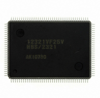
Manufacturer Part Number
D12321VF25V
Description
IC H8S/2300 MCU ROMLESS 128QFP
Manufacturer
Renesas Electronics America
Series
H8® H8S/2300r
Datasheets
1.HEWH8E10A.pdf
(19 pages)
2.D12312SVTE25V.pdf
(341 pages)
3.D12322RVF25V.pdf
(1304 pages)
Specifications of D12321VF25V
Core Processor
H8S/2000
Core Size
16-Bit
Speed
25MHz
Connectivity
SCI, SmartCard
Peripherals
POR, PWM, WDT
Number Of I /o
86
Program Memory Type
ROMless
Ram Size
4K x 8
Voltage - Supply (vcc/vdd)
2.7 V ~ 3.6 V
Data Converters
A/D 8x10b; D/A 2x8b
Oscillator Type
Internal
Operating Temperature
-20°C ~ 75°C
Package / Case
128-QFP
For Use With
EDK2329 - DEV EVALUATION KIT H8S/2329
Lead Free Status / RoHS Status
Lead free / RoHS Compliant
Eeprom Size
-
Program Memory Size
-
Available stocks
Company
Part Number
Manufacturer
Quantity
Price
Company:

Part Number:
D12321VF25V
Manufacturer:
Renesas Electronics America
Quantity:
135
Company:
Part Number:
D12321VF25V
Manufacturer:
Renesas
Quantity:
675
Company:
Part Number:
D12321VF25V
Manufacturer:
Renesas Electronics America
Quantity:
10 000


Section 15 Smart Card Interface
15.3.4
Table 15.3 shows a bit map of the registers used by the smart card interface.
Bits indicated as 0 or 1 must be set to the value shown. The setting of other bits is described
below.
Table 15.3 Smart Card Interface Register Settings
Register
SMR
BRR
SCR
TDR
SSR
RDR
SCMR
Notes: — : Unused bit.
SMR Settings: The GM bit is cleared to 0 in normal smart card interface mode, and set to 1 in
GSM mode. The O/E bit is cleared to 0 if the IC card is of the direct convention type, and set to 1
if of the inverse convention type.
Bits CKS1 and CKS0 select the clock source of the built-in baud rate generator, and bits BCP1
and BCP0 select the number of base clock cycles during transfer of one bit. For details, see section
15.3.5, Clock.
The BLK bit is cleared to 0 when using the normal smart card interface mode, and set to 1 when
using block transfer mode.
BRR Setting: BRR is used to set the bit rate. See section 15.3.5, Clock, for the method of
calculating the value to be set.
SCR Settings: The function of the TIE, RIE, TE, and RE bits is the same as for the normal SCI.
For details, see section 14, Serial Communication Interface (SCI).
Bits CKE1 and CKE0 specify the clock output. When the GM bit in SMR is cleared to 0, set these
bits to B'00 if a clock is not to be output, or to B'01 if a clock is to be output. When the GM bit in
SMR is set to 1, clock output is performed. The clock output can also be fixed high or low.
Rev.6.00 Sep. 27, 2007 Page 682 of 1268
REJ09B0220-0600
* The CKE1 bit must be cleared to 0 when the GM bit in SMR is cleared to 0.
Register Settings
Bit 7
GM
BRR7
TIE
TDR7
TDRE
RDR7
—
Bit 6
BLK
BRR6
RIE
TDR6
RDRF
RDR6
—
Bit 5
1
BRR5
TE
TDR5
ORER
RDR5
—
Bit 4
O/E
BRR4
RE
TDR4
ERS
RDR4
—
Bit
Bit 3
BCP1
BRR3
0
TDR3
PER
RDR3
SDIR
Bit 2
BCP0
BRR2
0
TDR2
TEND
RDR2
SINV
Bit 1
CKS1
BRR1
CKE1 *
TDR1
0
RDR1
—
Bit 0
CKS0
BRR0
CKE0
TDR0
0
RDR0
SMIF
Related parts for D12321VF25V
Image
Part Number
Description
Manufacturer
Datasheet
Request
R

Part Number:
Description:
KIT STARTER FOR M16C/29
Manufacturer:
Renesas Electronics America
Datasheet:

Part Number:
Description:
KIT STARTER FOR R8C/2D
Manufacturer:
Renesas Electronics America
Datasheet:

Part Number:
Description:
R0K33062P STARTER KIT
Manufacturer:
Renesas Electronics America
Datasheet:

Part Number:
Description:
KIT STARTER FOR R8C/23 E8A
Manufacturer:
Renesas Electronics America
Datasheet:

Part Number:
Description:
KIT STARTER FOR R8C/25
Manufacturer:
Renesas Electronics America
Datasheet:

Part Number:
Description:
KIT STARTER H8S2456 SHARPE DSPLY
Manufacturer:
Renesas Electronics America
Datasheet:

Part Number:
Description:
KIT STARTER FOR R8C38C
Manufacturer:
Renesas Electronics America
Datasheet:

Part Number:
Description:
KIT STARTER FOR R8C35C
Manufacturer:
Renesas Electronics America
Datasheet:

Part Number:
Description:
KIT STARTER FOR R8CL3AC+LCD APPS
Manufacturer:
Renesas Electronics America
Datasheet:
Part Number:
Description:
KIT STARTER FOR RX610
Manufacturer:
Renesas Electronics America
Datasheet:

Part Number:
Description:
KIT STARTER FOR R32C/118
Manufacturer:
Renesas Electronics America
Datasheet:

Part Number:
Description:
KIT DEV RSK-R8C/26-29
Manufacturer:
Renesas Electronics America
Datasheet:

Part Number:
Description:
KIT STARTER FOR SH7124
Manufacturer:
Renesas Electronics America
Datasheet:

Part Number:
Description:
KIT STARTER FOR H8SX/1622
Manufacturer:
Renesas Electronics America
Datasheet:

Part Number:
Description:
KIT DEV FOR SH7203
Manufacturer:
Renesas Electronics America
Datasheet: