EFM32G200F16 Energy Micro, EFM32G200F16 Datasheet - Page 457
EFM32G200F16
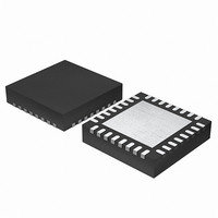
Manufacturer Part Number
EFM32G200F16
Description
MCU 32BIT 16KB FLASH 32-QFN
Manufacturer
Energy Micro
Series
Geckor
Datasheets
1.EFM32G200F16.pdf
(63 pages)
2.EFM32G200F16.pdf
(10 pages)
3.EFM32G200F16.pdf
(463 pages)
4.EFM32G200F16.pdf
(136 pages)
Specifications of EFM32G200F16
Core Processor
ARM® Cortex-M3™
Core Size
32-Bit
Speed
32MHz
Connectivity
EBI/EMI, I²C, IrDA, SmartCard, SPI, UART/USART
Peripherals
Brown-out Detect/Reset, DMA, POR, PWM, WDT
Number Of I /o
24
Program Memory Size
16KB (16K x 8)
Program Memory Type
FLASH
Ram Size
8K x 8
Voltage - Supply (vcc/vdd)
1.8 V ~ 3.8 V
Data Converters
A/D 4x12b, D/A 1x12b
Oscillator Type
External
Operating Temperature
-40°C ~ 85°C
Package / Case
32-VQFN Exposed Pad
Processor Series
EFM32G200
Core
ARM Cortex-M3
Data Bus Width
32 bit
Data Ram Size
8 KB
Interface Type
I2C, UART
Maximum Clock Frequency
32 MHz
Number Of Programmable I/os
24
Number Of Timers
2
Operating Supply Voltage
1.8 V to 3.8 V
Maximum Operating Temperature
+ 85 C
Mounting Style
SMD/SMT
Minimum Operating Temperature
- 40 C
Lead Free Status / RoHS Status
Lead free / RoHS Compliant
Eeprom Size
-
Lead Free Status / Rohs Status
Details


...the world's most energy friendly microcontrollers
19.1. TIMER Block Overview ....................................................................................................................... 244
19.2. TIMER Hardware Timer/Counter Control ................................................................................................ 245
19.3. TIMER Clock Selection ....................................................................................................................... 245
19.4. TIMER Connections ........................................................................................................................... 246
19.5. TIMER TOP Value Update Functionality ................................................................................................. 246
19.6. TIMER Quadrature Encoded Inputs ....................................................................................................... 247
19.7. TIMER Quadrature Decoder Configuration .............................................................................................. 247
19.8. TIMER X2 Decoding Mode .................................................................................................................. 248
19.9. TIMER X4 Decoding Mode .................................................................................................................. 248
19.10. TIMER Input Pin Logic ...................................................................................................................... 249
19.11. TIMER Input Capture Buffer Functionality ............................................................................................. 249
19.12. TIMER Output Compare/PWM Buffer Functionality ................................................................................. 250
19.13. TIMER Input Capture ........................................................................................................................ 250
19.14. TIMER Period and/or Pulse width Capture ............................................................................................ 251
19.15. TIMER Block Diagram Showing Comparison Functionality ........................................................................ 251
19.16. TIMER Output Logic ......................................................................................................................... 251
19.17. TIMER Up-count Frequency Generation ............................................................................................... 252
19.18. TIMER Up-count PWM Generation ...................................................................................................... 252
19.19. TIMER Up/Down-count PWM Generation .............................................................................................. 253
19.20. TIMER Dead-Time Insertion Unit Overview ........................................................................................... 253
19.21. TIMER Triple Half-Bridge ................................................................................................................... 254
19.22. TIMER Overview of Dead-Time Insertion Block for a Single PWM channel .................................................. 254
19.23. TIMER Polarity of Both Signals are Set as Active-High ............................................................................ 254
19.24. TIMER Output Polarities .................................................................................................................... 255
20.1. RTC Overview ................................................................................................................................... 277
21.1. LETIMER Overview ............................................................................................................................ 286
21.2. LETIMER State Machine for Free-running Mode ...................................................................................... 288
21.3. LETIMER One-shot Repeat State Machine ............................................................................................. 289
21.4. LETIMER Buffered Repeat State Machine .............................................................................................. 290
21.5. LETIMER Double Repeat State Machine ................................................................................................ 291
21.6. LETIMER Simple Waveforms Output ..................................................................................................... 293
21.7. LETIMER Repeated Counting .............................................................................................................. 293
21.8. LETIMER Dual Output ........................................................................................................................ 293
21.9. LETIMER Triggered Operation ............................................................................................................. 294
21.10. LETIMER Continuous Operation ......................................................................................................... 295
21.11. LETIMER LETIMERn_CNT Not Initialized to 0 ....................................................................................... 296
22.1. PCNT Overview ................................................................................................................................. 308
22.2. PCNT Quadrature Coding ................................................................................................................... 309
22.3. PCNT Direction Change Interrupt (DIRCNG) Generation ........................................................................... 312
23.1. ACMP Overview ................................................................................................................................ 321
23.2. 20 mV Hysteresis Selected .................................................................................................................. 323
23.3. Capacitive Sensing Set-up ................................................................................................................... 324
24.1. VCMP Overview ................................................................................................................................ 332
24.2. VCMP 20 mV Hysteresis Enabled ......................................................................................................... 333
25.1. ADC Overview .................................................................................................................................. 341
25.2. ADC Conversion Timing ...................................................................................................................... 342
25.3. ADC RC Input Filter Configuration ........................................................................................................ 343
25.4. ADC Bias Programming ...................................................................................................................... 344
25.5. ADC Conversion Tailgating .................................................................................................................. 345
26.1. DAC Overview .................................................................................................................................. 363
26.2. DAC Bias Programming ...................................................................................................................... 365
26.3. DAC Sine Mode ................................................................................................................................ 366
27.1. AES Key and Data Definitions .............................................................................................................. 378
27.2. AES Data and Key Orientation as Defined in the Advanced Encryption Standard ............................................ 378
27.3. AES Data and Key Register Operation .................................................................................................. 379
28.1. Pin Configuration ............................................................................................................................... 391
28.2. Tristated Output with Optional Pull-up or Pull-down .................................................................................. 392
28.3. Push-Pull Configuration ....................................................................................................................... 393
28.4. Open-drain ....................................................................................................................................... 393
28.5. Pin n Interrupt Generation ................................................................................................................... 394
29.1. LCD Block Diagram ........................................................................................................................... 412
29.2. LCD Low-power Waveform for LCD_COM0 in Quadruples Multiplex Mode, 1/3 Bias ........................................ 413
29.3. LCD Normal Waveform for LCD_COM0 in Quadruples Multiplex Mode, 1/3 Bias ............................................ 414
29.4. LCD Static Bias and Multiplexing - LCD_COM0 ....................................................................................... 414
29.5. LCD 1/2 Bias and Duplex Multiplexing - LCD_COM0 ................................................................................ 414
29.6. LCD 1/2 Bias and Duplex Multiplexing - LCD_COM1 ................................................................................ 415
29.7. LCD 1/2 Bias and Duplex Multiplexing - LCD_SEG0 ................................................................................. 415
29.8. LCD 1/2 Bias and Duplex Multiplexing - LCD_SEG0 Connection ................................................................. 415
29.9. LCD 1/2 Bias and Duplex Multiplexing - LCD_SEG0-LCD_COM0 ................................................................ 415
29.10. LCD 1/2 Bias and Duplex Multiplexing - LCD_SEG0-LCD_COM1 .............................................................. 416
29.11. LCD 1/3 Bias and Duplex Multiplexing - LCD_COM0 .............................................................................. 416
29.12. LCD 1/3 Bias and Duplex Multiplexing - LCD_COM1 .............................................................................. 416
29.13. LCD 1/3 Bias and Duplex Multiplexing - LCD_SEG0 ............................................................................... 416
29.14. LCD 1/3 Bias and Duplex Multiplexing - LCD_SEG0 Connection ............................................................... 417
www.energymicro.com
2010-09-06 - d0001_Rev1.00
457
Related parts for EFM32G200F16
Image
Part Number
Description
Manufacturer
Datasheet
Request
R

Part Number:
Description:
KIT STARTER EFM32 GECKO
Manufacturer:
Energy Micro
Datasheet:

Part Number:
Description:
KIT DEV EFM32 GECKO LCD SUPPORT
Manufacturer:
Energy Micro
Datasheet:

Part Number:
Description:
BOARD PROTOTYPING FOR EFM32
Manufacturer:
Energy Micro
Datasheet:

Part Number:
Description:
KIT DEVELOPMENT EFM32 GECKO
Manufacturer:
Energy Micro
Datasheet:

Part Number:
Description:
MCU, MPU & DSP Development Tools TG840 Sample Kit
Manufacturer:
Energy Micro
Datasheet:

Part Number:
Description:
MCU, MPU & DSP Development Tools TG Starter Kit
Manufacturer:
Energy Micro
Datasheet:
Part Number:
Description:
MCU, MPU & DSP Development Tools TG108 Sample Kit
Manufacturer:
Energy Micro
Part Number:
Description:
MCU, MPU & DSP Development Tools TG210 Sample Kit
Manufacturer:
Energy Micro
Datasheet:
Part Number:
Description:
MCU, MPU & DSP Development Tools TG822 Sample Kit
Manufacturer:
Energy Micro
Datasheet:
Part Number:
Description:
MCU, MPU & DSP Development Tools TG230 Sample Kit
Manufacturer:
Energy Micro

Part Number:
Description:
SAMPLE KIT (SMALL BOX - CONTAINING 2 DEVICES)
Manufacturer:
Energy Micro
Part Number:
Description:
SAMPLE KIT (SMALL BOX - CONTAINING 2 DEVICES)
Manufacturer:
Energy Micro