EFM32G200F16 Energy Micro, EFM32G200F16 Datasheet - Page 459
EFM32G200F16
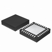
Manufacturer Part Number
EFM32G200F16
Description
MCU 32BIT 16KB FLASH 32-QFN
Manufacturer
Energy Micro
Series
Geckor
Datasheets
1.EFM32G200F16.pdf
(63 pages)
2.EFM32G200F16.pdf
(10 pages)
3.EFM32G200F16.pdf
(463 pages)
4.EFM32G200F16.pdf
(136 pages)
Specifications of EFM32G200F16
Core Processor
ARM® Cortex-M3™
Core Size
32-Bit
Speed
32MHz
Connectivity
EBI/EMI, I²C, IrDA, SmartCard, SPI, UART/USART
Peripherals
Brown-out Detect/Reset, DMA, POR, PWM, WDT
Number Of I /o
24
Program Memory Size
16KB (16K x 8)
Program Memory Type
FLASH
Ram Size
8K x 8
Voltage - Supply (vcc/vdd)
1.8 V ~ 3.8 V
Data Converters
A/D 4x12b, D/A 1x12b
Oscillator Type
External
Operating Temperature
-40°C ~ 85°C
Package / Case
32-VQFN Exposed Pad
Processor Series
EFM32G200
Core
ARM Cortex-M3
Data Bus Width
32 bit
Data Ram Size
8 KB
Interface Type
I2C, UART
Maximum Clock Frequency
32 MHz
Number Of Programmable I/os
24
Number Of Timers
2
Operating Supply Voltage
1.8 V to 3.8 V
Maximum Operating Temperature
+ 85 C
Mounting Style
SMD/SMT
Minimum Operating Temperature
- 40 C
Lead Free Status / RoHS Status
Lead free / RoHS Compliant
Eeprom Size
-
Lead Free Status / Rohs Status
Details


2010-09-06 - d0001_Rev1.00
List of Tables
2.1. Register Access Types ............................................................................................................................ 3
3.1. Energy Mode Description ......................................................................................................................... 8
3.2. EFM32G Microcontroller Family ................................................................................................................. 9
4.1. Interrupt Request Lines (IRQ) .................................................................................................................. 12
5.1. Memory System Core Peripherals ............................................................................................................ 15
5.2. Memory System Low Energy Peripherals ................................................................................................... 16
5.3. Memory System Peripherals .................................................................................................................... 17
5.4. Device Information Table ........................................................................................................................ 21
7.1. MSC Flash Memory Mapping .................................................................................................................. 28
7.2. Lock Bits Page Structure ........................................................................................................................ 29
7.3. Revision Number Interpretation ................................................................................................................ 30
8.1. AHB bus transfer arbitration interval ......................................................................................................... 40
8.2. DMA channel priority ............................................................................................................................. 41
8.3. DMA cycle types ................................................................................................................................... 42
8.4. channel_cfg for a primary data structure, in memory scatter-gather mode ......................................................... 46
8.5. channel_cfg for a primary data structure, in peripheral scatter-gather mode ...................................................... 48
8.6. Address bit settings for the channel control data structure ............................................................................. 51
8.7. src_data_end_ptr bit assignments ............................................................................................................ 52
8.8. dst_data_end_ptr bit assignments ............................................................................................................ 53
8.9. channel_cfg bit assignments ................................................................................................................... 53
8.10. DMA cycle of six words using a word increment ........................................................................................ 56
8.11. DMA cycle of 12 bytes using a halfword increment .................................................................................... 57
9.1. RMU Reset Cause Register Interpretation ................................................................................................. 76
10.1. EMU Energy Mode Overview ................................................................................................................. 84
10.2. EMU Entering a Low Energy Mode ......................................................................................................... 85
10.3. EMU Wakeup Triggers from Low Energy Modes ....................................................................................... 86
13.1. Reflex Producers ............................................................................................................................... 125
13.2. Reflex Consumers ............................................................................................................................. 126
14.1. EBI Timing ....................................................................................................................................... 136
15.1. I
15.2. I
15.3. I
15.4. I
15.5. I
15.6. I
15.7. I
15.8. I
15.9. I
15.10. I
16.1. USART Asynchronous vs. Synchronous Mode ........................................................................................ 177
16.2. USART Pin Usage ............................................................................................................................. 177
16.3. USART Data Bits ............................................................................................................................... 178
16.4. USART Stop Bits ............................................................................................................................... 178
16.5. USART Parity Bits ............................................................................................................................. 179
16.6. USART Oversampling ......................................................................................................................... 179
16.7. USART Baud Rates @ 4MHz Peripheral Clock ....................................................................................... 180
16.8. USART SPI Modes ............................................................................................................................ 192
16.9. USART IrDA Pulse Widths .................................................................................................................. 196
17.1. UART Limitations ............................................................................................................................... 216
18.1. LEUART Parity Bit ............................................................................................................................. 219
18.2. LEUART Baud Rates ......................................................................................................................... 220
19.1. TIMER Counter Response in X2 Decoding Mode ..................................................................................... 248
19.2. TIMER Counter Response in X4 Decoding Mode ..................................................................................... 248
19.3. TIMER Events ................................................................................................................................... 257
20.1. RTC Resolution Vs Overflow ............................................................................................................... 278
21.1. LETIMER Repeat Modes ..................................................................................................................... 287
21.2. LETIMER Underflow Output Actions ...................................................................................................... 292
22.1. PCNT QUAD Mode Counter Control Function ......................................................................................... 310
23.1. Bias Configuration .............................................................................................................................. 322
24.1. Bias Configuration .............................................................................................................................. 332
25.1. ADC Single Ended Conversion ............................................................................................................. 345
25.2. ADC Differential Conversion ................................................................................................................ 346
25.3. Oversampling Result Shifting and Resolution .......................................................................................... 346
25.4. ADC Results Representation ................................................................................................................ 347
25.5. Calibration Register Effect ................................................................................................................... 348
28.1. Pin Configuration ............................................................................................................................... 391
29.1. LCD Mux Settings .............................................................................................................................. 413
29.2. LCD BIAS Settings ............................................................................................................................ 413
29.3. LCD Wave Settings ............................................................................................................................ 413
29.4. LCD Contrast .................................................................................................................................... 424
29.5. LCD Contrast Function ....................................................................................................................... 424
2
2
2
2
2
2
2
2
2
C Reserved I
C Clock Modes ............................................................................................................................... 147
C Interactions in Prioritized Order ....................................................................................................... 150
C Master Transmitter ........................................................................................................................ 152
C Master Receiver ........................................................................................................................... 154
C STATE Values ............................................................................................................................. 155
C Transmission Status ...................................................................................................................... 155
C Slave Transmitter ......................................................................................................................... 158
C - Slave Receiver .......................................................................................................................... 159
2
C Bus Error Response .................................................................................................................... 160
2
C Addresses ................................................................................................................ 145
...the world's most energy friendly microcontrollers
459
www.energymicro.com
Related parts for EFM32G200F16
Image
Part Number
Description
Manufacturer
Datasheet
Request
R

Part Number:
Description:
KIT STARTER EFM32 GECKO
Manufacturer:
Energy Micro
Datasheet:

Part Number:
Description:
KIT DEV EFM32 GECKO LCD SUPPORT
Manufacturer:
Energy Micro
Datasheet:

Part Number:
Description:
BOARD PROTOTYPING FOR EFM32
Manufacturer:
Energy Micro
Datasheet:

Part Number:
Description:
KIT DEVELOPMENT EFM32 GECKO
Manufacturer:
Energy Micro
Datasheet:

Part Number:
Description:
MCU, MPU & DSP Development Tools TG840 Sample Kit
Manufacturer:
Energy Micro
Datasheet:

Part Number:
Description:
MCU, MPU & DSP Development Tools TG Starter Kit
Manufacturer:
Energy Micro
Datasheet:
Part Number:
Description:
MCU, MPU & DSP Development Tools TG108 Sample Kit
Manufacturer:
Energy Micro
Part Number:
Description:
MCU, MPU & DSP Development Tools TG210 Sample Kit
Manufacturer:
Energy Micro
Datasheet:
Part Number:
Description:
MCU, MPU & DSP Development Tools TG822 Sample Kit
Manufacturer:
Energy Micro
Datasheet:
Part Number:
Description:
MCU, MPU & DSP Development Tools TG230 Sample Kit
Manufacturer:
Energy Micro

Part Number:
Description:
SAMPLE KIT (SMALL BOX - CONTAINING 2 DEVICES)
Manufacturer:
Energy Micro
Part Number:
Description:
SAMPLE KIT (SMALL BOX - CONTAINING 2 DEVICES)
Manufacturer:
Energy Micro