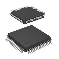
DF71251AD50FPV Renesas Electronics America, DF71251AD50FPV Datasheet - Page 157

DF71251AD50FPV
Manufacturer Part Number
DF71251AD50FPV
Description
MCU RISC FLASH 32K 8K 64LQFP
Manufacturer
Renesas Electronics America
Series
SuperH® SH Tinyr
Datasheet
1.DF71243N50FPV.pdf
(794 pages)
Specifications of DF71251AD50FPV
Core Processor
SH-2
Core Size
32-Bit
Speed
50MHz
Connectivity
SCI
Peripherals
POR, PWM, WDT
Number Of I /o
37
Program Memory Size
32KB (32K x 8)
Program Memory Type
FLASH
Ram Size
8K x 8
Voltage - Supply (vcc/vdd)
4 V ~ 5.5 V
Data Converters
A/D 8x10b
Oscillator Type
External
Operating Temperature
-40°C ~ 85°C
Package / Case
64-LQFP
Lead Free Status / RoHS Status
Lead free / RoHS Compliant
Eeprom Size
-
Available stocks
Company
Part Number
Manufacturer
Quantity
Price
Company:
Part Number:
DF71251AD50FPV
Manufacturer:
Renesas Electronics America
Quantity:
10 000
- Current page: 157 of 794
- Download datasheet (5Mb)
7.3.2
1. When L bus/instruction fetch/read/word, longword, or not including the operand size is set in
2. An instruction set for a break before execution breaks when it is confirmed that the instruction
3. When the condition is specified to be occur after execution, the instruction set with the break
4. When an instruction fetch cycle is set, the break data register (BDRA or BDRB) is ignored.
5. If the I bus is set for a break of an instruction fetch cycle, the condition is determined for the
7.3.3
1. If the L bus is specified as a break condition for data access break, condition comparison is
2. The relationship between the data access cycle address and the comparison condition for each
the break bus cycle register (BBRA or BBRB), the break condition becomes the L bus
instruction fetch cycle. Whether it breaks before or after the execution of the instruction can
then be selected with the PCBA or PCBB bit in the break control register (BRCR) for the
appropriate channel. If an instruction fetch cycle is set as a break condition, clear LSB in the
break address register (BARA or BARB) to 0. A break cannot be generated as long as this bit
is set to 1.
has been fetched and will be executed. This means this feature cannot be used on instructions
fetched by overrun (instructions fetched at a branch or during an interrupt transition, but not to
be executed). When this kind of break is set for the delay slot of a delayed branch instruction,
the break is generated prior to execution of the delayed branch instruction.
condition is executed and then the break is generated prior to the execution of the next
instruction. As with pre-execution breaks, this cannot be used with overrun fetch instructions.
When this kind of break is set for a delayed branch instruction and its delay slot, a break is not
generated until the first instruction at the branch destination.
Therefore, break data cannot be set for the break of the instruction fetch cycle.
instruction fetch cycles on the I bus. For details, see 5 in section 7.3.1, Flow of the User Break
Operation.
performed for the address (and data) accessed by the executed instructions, and a break occurs
if the condition is satisfied. If the I bus is specified as a break condition, condition comparison
is performed for the addresses (and data) of the data access cycles that are issued on the I bus
by all bus masters including the CPU, and a break occurs if the condition is satisfied. For
details on the CPU bus cycles issued on the I bus, see 5 in section 7.3.1, Flow of the User
Break Operation.
operand size is listed in table 7.2.
Note: If a branch does not occur at a delay condition branch instruction, the subsequent
Break on Instruction Fetch Cycle
Break on Data Access Cycle
instruction is not recognized as a delay slot.
Rev. 5.00 Mar. 06, 2009 Page 137 of 770
REJ09B0243-0500
Related parts for DF71251AD50FPV
Image
Part Number
Description
Manufacturer
Datasheet
Request
R

Part Number:
Description:
KIT STARTER FOR M16C/29
Manufacturer:
Renesas Electronics America
Datasheet:

Part Number:
Description:
KIT STARTER FOR R8C/2D
Manufacturer:
Renesas Electronics America
Datasheet:

Part Number:
Description:
R0K33062P STARTER KIT
Manufacturer:
Renesas Electronics America
Datasheet:

Part Number:
Description:
KIT STARTER FOR R8C/23 E8A
Manufacturer:
Renesas Electronics America
Datasheet:

Part Number:
Description:
KIT STARTER FOR R8C/25
Manufacturer:
Renesas Electronics America
Datasheet:

Part Number:
Description:
KIT STARTER H8S2456 SHARPE DSPLY
Manufacturer:
Renesas Electronics America
Datasheet:

Part Number:
Description:
KIT STARTER FOR R8C38C
Manufacturer:
Renesas Electronics America
Datasheet:

Part Number:
Description:
KIT STARTER FOR R8C35C
Manufacturer:
Renesas Electronics America
Datasheet:

Part Number:
Description:
KIT STARTER FOR R8CL3AC+LCD APPS
Manufacturer:
Renesas Electronics America
Datasheet:

Part Number:
Description:
KIT STARTER FOR RX610
Manufacturer:
Renesas Electronics America
Datasheet:

Part Number:
Description:
KIT STARTER FOR R32C/118
Manufacturer:
Renesas Electronics America
Datasheet:

Part Number:
Description:
KIT DEV RSK-R8C/26-29
Manufacturer:
Renesas Electronics America
Datasheet:

Part Number:
Description:
KIT STARTER FOR SH7124
Manufacturer:
Renesas Electronics America
Datasheet:

Part Number:
Description:
KIT STARTER FOR H8SX/1622
Manufacturer:
Renesas Electronics America
Datasheet:

Part Number:
Description:
KIT DEV FOR SH7203
Manufacturer:
Renesas Electronics America
Datasheet:


