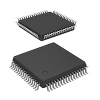
DF71251AD50FPV Renesas Electronics America, DF71251AD50FPV Datasheet - Page 341

DF71251AD50FPV
Manufacturer Part Number
DF71251AD50FPV
Description
MCU RISC FLASH 32K 8K 64LQFP
Manufacturer
Renesas Electronics America
Series
SuperH® SH Tinyr
Datasheet
1.DF71243N50FPV.pdf
(794 pages)
Specifications of DF71251AD50FPV
Core Processor
SH-2
Core Size
32-Bit
Speed
50MHz
Connectivity
SCI
Peripherals
POR, PWM, WDT
Number Of I /o
37
Program Memory Size
32KB (32K x 8)
Program Memory Type
FLASH
Ram Size
8K x 8
Voltage - Supply (vcc/vdd)
4 V ~ 5.5 V
Data Converters
A/D 8x10b
Oscillator Type
External
Operating Temperature
-40°C ~ 85°C
Package / Case
64-LQFP
Lead Free Status / RoHS Status
Lead free / RoHS Compliant
Eeprom Size
-
Available stocks
Company
Part Number
Manufacturer
Quantity
Price
Company:
Part Number:
DF71251AD50FPV
Manufacturer:
Renesas Electronics America
Quantity:
10 000
- Current page: 341 of 794
- Download datasheet (5Mb)
9.5.2
The A/D converter can be activated by one of the following three methods in the MTU2. Table
9.58 shows the relationship between interrupt sources and A/D converter start request signals.
A/D Converter Activation by TGRA Input Capture/Compare Match or at TCNT_4 Trough
in Complementary PWM Mode: The A/D converter can be activated by the occurrence of a
TGRA input capture/compare match in each channel. In addition, if complementary PWM
operation is performed while the TTGE2 bit in TIER_4 is set to 1, the A/D converter can be
activated at the trough of TCNT_4 count (TCNT_4 = H'0000).
A/D converter start request signal TRGAN is issued to the A/D converter under either one of the
following conditions.
• When the TGFA flag in TSR is set to 1 by the occurrence of a TGRA input capture/compare
• When the TCNT_4 count reaches the trough (TCNT_4 = H'0000) during complementary
When either condition is satisfied, if A/D converter start signal TRGAN from the MTU2 is
selected as the trigger in the A/D converter, A/D conversion will start.
A/D Converter Activation by Compare Match between TCNT_0 and TGRE_0: The A/D
converter can be activated by generating A/D converter start request signal TRG0N when a
compare match occurs between TCNT_0 and TGRE_0 in channel 0.
When the TGFE flag in TSR2_0 is set to 1 by the occurrence of a compare match between
TCNT_0 and TGRE_0 in channel 0 while the TTGE2 bit in TIER2_0 is set to 1, A/D converter
start request TGR0N is issued to the A/D converter. If A/D converter start signal TGR0N from the
MTU2 is selected as the trigger in the A/D converter, A/D conversion will start.
A/D Converter Activation by A/D Converter Start Request Delaying Function: The A/D
converter can be activated by generating A/D converter start request signal TRG4AN or TRG4BN
when the TCNT_4 count matches the TADCORA or TADCORB value if the UT4AE, DT4AE,
UT4BE, or DT4BE bit in the A/D converter start request control register (TADCR) is set to 1. For
details, refer to section 9.4.9, A/D Converter Start Request Delaying Function.
A/D conversion will start if A/D converter start signal TRG4AN from the MTU2 is selected as the
trigger in the A/D converter when TRG4AN is generated or if TRG4BN from the MTU2 is
selected as the trigger in the A/D converter when TRG4BN is generated.
match on a particular channel while the TTGE bit in TIER is set to 1
PWM operation while the TTGE2 bit in TIER_4 is set to 1
A/D Converter Activation
Rev. 5.00 Mar. 06, 2009 Page 321 of 770
REJ09B0243-0500
Related parts for DF71251AD50FPV
Image
Part Number
Description
Manufacturer
Datasheet
Request
R

Part Number:
Description:
KIT STARTER FOR M16C/29
Manufacturer:
Renesas Electronics America
Datasheet:

Part Number:
Description:
KIT STARTER FOR R8C/2D
Manufacturer:
Renesas Electronics America
Datasheet:

Part Number:
Description:
R0K33062P STARTER KIT
Manufacturer:
Renesas Electronics America
Datasheet:

Part Number:
Description:
KIT STARTER FOR R8C/23 E8A
Manufacturer:
Renesas Electronics America
Datasheet:

Part Number:
Description:
KIT STARTER FOR R8C/25
Manufacturer:
Renesas Electronics America
Datasheet:

Part Number:
Description:
KIT STARTER H8S2456 SHARPE DSPLY
Manufacturer:
Renesas Electronics America
Datasheet:

Part Number:
Description:
KIT STARTER FOR R8C38C
Manufacturer:
Renesas Electronics America
Datasheet:

Part Number:
Description:
KIT STARTER FOR R8C35C
Manufacturer:
Renesas Electronics America
Datasheet:

Part Number:
Description:
KIT STARTER FOR R8CL3AC+LCD APPS
Manufacturer:
Renesas Electronics America
Datasheet:

Part Number:
Description:
KIT STARTER FOR RX610
Manufacturer:
Renesas Electronics America
Datasheet:

Part Number:
Description:
KIT STARTER FOR R32C/118
Manufacturer:
Renesas Electronics America
Datasheet:

Part Number:
Description:
KIT DEV RSK-R8C/26-29
Manufacturer:
Renesas Electronics America
Datasheet:

Part Number:
Description:
KIT STARTER FOR SH7124
Manufacturer:
Renesas Electronics America
Datasheet:

Part Number:
Description:
KIT STARTER FOR H8SX/1622
Manufacturer:
Renesas Electronics America
Datasheet:

Part Number:
Description:
KIT DEV FOR SH7203
Manufacturer:
Renesas Electronics America
Datasheet:


