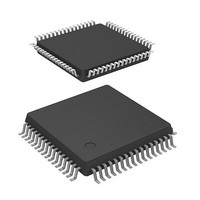
DF71251AD50FPV Renesas Electronics America, DF71251AD50FPV Datasheet - Page 173

DF71251AD50FPV
Manufacturer Part Number
DF71251AD50FPV
Description
MCU RISC FLASH 32K 8K 64LQFP
Manufacturer
Renesas Electronics America
Series
SuperH® SH Tinyr
Datasheet
1.DF71243N50FPV.pdf
(794 pages)
Specifications of DF71251AD50FPV
Core Processor
SH-2
Core Size
32-Bit
Speed
50MHz
Connectivity
SCI
Peripherals
POR, PWM, WDT
Number Of I /o
37
Program Memory Size
32KB (32K x 8)
Program Memory Type
FLASH
Ram Size
8K x 8
Voltage - Supply (vcc/vdd)
4 V ~ 5.5 V
Data Converters
A/D 8x10b
Oscillator Type
External
Operating Temperature
-40°C ~ 85°C
Package / Case
64-LQFP
Lead Free Status / RoHS Status
Lead free / RoHS Compliant
Eeprom Size
-
Available stocks
Company
Part Number
Manufacturer
Quantity
Price
Company:
Part Number:
DF71251AD50FPV
Manufacturer:
Renesas Electronics America
Quantity:
10 000
- Current page: 173 of 794
- Download datasheet (5Mb)
This LSI has an on-chip multi-function timer pulse unit 2 (MTU2) that comprises six 16-bit timer
channels.
9.1
• Maximum 16 (SH7125) or 12 (SH7124) pulse input/output lines and three pulse input lines
• Selection of eight counter input clocks for each channel (four clocks for channel 5)
• The following operations can be set for channels 0 to 4:
• Buffer operation settable for channels 0, 3, and 4
• Phase counting mode settable independently for each of channels 1 and 2
• Cascade connection operation
• Fast access via internal 16-bit bus
• 28 interrupt sources
• Automatic transfer of register data
• A/D converter start trigger can be generated
• Module standby mode can be settable
• A total of six-phase waveform output, which includes complementary PWM output, and
• AC synchronous motor (brushless DC motor) drive mode using complementary PWM output
• Dead time compensation counter available in channel 5
• In complementary PWM mode, interrupts at the crest and trough of the counter value and A/D
TIMMTU1A_020020030800
⎯ Waveform output at compare match
⎯ Input capture function
⎯ Counter clear operation
⎯ Multiple timer counters (TCNT) can be written to simultaneously
⎯ Simultaneous clearing by compare match and input capture is possible
⎯ Register simultaneous input/output is possible by synchronous counter operation
⎯ A maximum 12-phase PWM output is possible in combination with synchronous operation
positive and negative phases of reset PWM output by interlocking operation of channels 3 and
4, is possible.
and reset PWM output is settable by interlocking operation of channels 0, 3, and 4, and the
selection of two types of waveform outputs (chopping and level) is possible.
converter start triggers can be skipped.
Section 9 Multi-Function Timer Pulse Unit 2 (MTU2)
Features
Rev. 5.00 Mar. 06, 2009 Page 153 of 770
REJ09B0243-0500
Related parts for DF71251AD50FPV
Image
Part Number
Description
Manufacturer
Datasheet
Request
R

Part Number:
Description:
KIT STARTER FOR M16C/29
Manufacturer:
Renesas Electronics America
Datasheet:

Part Number:
Description:
KIT STARTER FOR R8C/2D
Manufacturer:
Renesas Electronics America
Datasheet:

Part Number:
Description:
R0K33062P STARTER KIT
Manufacturer:
Renesas Electronics America
Datasheet:

Part Number:
Description:
KIT STARTER FOR R8C/23 E8A
Manufacturer:
Renesas Electronics America
Datasheet:

Part Number:
Description:
KIT STARTER FOR R8C/25
Manufacturer:
Renesas Electronics America
Datasheet:

Part Number:
Description:
KIT STARTER H8S2456 SHARPE DSPLY
Manufacturer:
Renesas Electronics America
Datasheet:

Part Number:
Description:
KIT STARTER FOR R8C38C
Manufacturer:
Renesas Electronics America
Datasheet:

Part Number:
Description:
KIT STARTER FOR R8C35C
Manufacturer:
Renesas Electronics America
Datasheet:

Part Number:
Description:
KIT STARTER FOR R8CL3AC+LCD APPS
Manufacturer:
Renesas Electronics America
Datasheet:

Part Number:
Description:
KIT STARTER FOR RX610
Manufacturer:
Renesas Electronics America
Datasheet:

Part Number:
Description:
KIT STARTER FOR R32C/118
Manufacturer:
Renesas Electronics America
Datasheet:

Part Number:
Description:
KIT DEV RSK-R8C/26-29
Manufacturer:
Renesas Electronics America
Datasheet:

Part Number:
Description:
KIT STARTER FOR SH7124
Manufacturer:
Renesas Electronics America
Datasheet:

Part Number:
Description:
KIT STARTER FOR H8SX/1622
Manufacturer:
Renesas Electronics America
Datasheet:

Part Number:
Description:
KIT DEV FOR SH7203
Manufacturer:
Renesas Electronics America
Datasheet:


