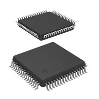
DF71251AD50FPV Renesas Electronics America, DF71251AD50FPV Datasheet - Page 433

DF71251AD50FPV
Manufacturer Part Number
DF71251AD50FPV
Description
MCU RISC FLASH 32K 8K 64LQFP
Manufacturer
Renesas Electronics America
Series
SuperH® SH Tinyr
Datasheet
1.DF71243N50FPV.pdf
(794 pages)
Specifications of DF71251AD50FPV
Core Processor
SH-2
Core Size
32-Bit
Speed
50MHz
Connectivity
SCI
Peripherals
POR, PWM, WDT
Number Of I /o
37
Program Memory Size
32KB (32K x 8)
Program Memory Type
FLASH
Ram Size
8K x 8
Voltage - Supply (vcc/vdd)
4 V ~ 5.5 V
Data Converters
A/D 8x10b
Oscillator Type
External
Operating Temperature
-40°C ~ 85°C
Package / Case
64-LQFP
Lead Free Status / RoHS Status
Lead free / RoHS Compliant
Eeprom Size
-
Available stocks
Company
Part Number
Manufacturer
Quantity
Price
Company:
Part Number:
DF71251AD50FPV
Manufacturer:
Renesas Electronics America
Quantity:
10 000
- Current page: 433 of 794
- Download datasheet (5Mb)
This LSI has three independent serial communication interface (SCI) channels. The SCI can
handle both asynchronous and clock synchronous serial communication. In asynchronous serial
communication mode, serial data communication can be carried out with standard asynchronous
communication chips such as a Universal Asynchronous Receiver/Transmitter (UART) or
Asynchronous Communication Interface Adapter (ACIA). A function is also provided for serial
communication between processors (multiprocessor communication function).
12.1
• Choice of asynchronous or clock synchronous serial communication mode
• Asynchronous mode (channels 0 to 2 in the SH7125, channels 0 to 2 in the SH7124):
• Clock synchronous mode (channels 0 to 2 in the SH7125, channels 0 and 2 in the SH7124):
• Full duplex communication: The transmitting and receiving sections are independent, so the
• On-chip baud rate generator with selectable bit rates
• Internal or external transmit/receive clock source: From either baud rate generator (internal
• Choice of LSB-first or MSB-first data transfer (except for 7-bit data in asynchronous mode)
⎯ Serial data communication is performed by start-stop in character units. The SCIF can
⎯ Data length: 7 or 8 bits
⎯ Stop bit length: 1 or 2 bits
⎯ Parity: Even, odd, or none
⎯ Multiprocessor communications
⎯ Receive error detection: Parity, overrun, and framing errors
⎯ Break detection: Break is detected by reading the RXD pin level directly when a framing
⎯ Serial data communication is synchronized with a clock signal. The SCIF can communicate
⎯ Data length: 8 bits
⎯ Receive error detection: Overrun errors
SCI can transmit and receive simultaneously. Both sections use double buffering, so high-
speed continuous data transfer is possible in both transmit and receive directions.
clock) or SCK pin (external clock)
communicate with a universal asynchronous receiver/transmitter (UART), an asynchronous
communication interface adapter (ACIA), or any other communications chip that employs
a standard asynchronous serial system. There are twelve selectable serial data
communication formats.
error occurs.
with other chips having a clock synchronous communication function.
Section 12 Serial Communication Interface (SCI)
Features
Rev. 5.00 Mar. 06, 2009 Page 413 of 770
REJ09B0243-0500
Related parts for DF71251AD50FPV
Image
Part Number
Description
Manufacturer
Datasheet
Request
R

Part Number:
Description:
KIT STARTER FOR M16C/29
Manufacturer:
Renesas Electronics America
Datasheet:

Part Number:
Description:
KIT STARTER FOR R8C/2D
Manufacturer:
Renesas Electronics America
Datasheet:

Part Number:
Description:
R0K33062P STARTER KIT
Manufacturer:
Renesas Electronics America
Datasheet:

Part Number:
Description:
KIT STARTER FOR R8C/23 E8A
Manufacturer:
Renesas Electronics America
Datasheet:

Part Number:
Description:
KIT STARTER FOR R8C/25
Manufacturer:
Renesas Electronics America
Datasheet:

Part Number:
Description:
KIT STARTER H8S2456 SHARPE DSPLY
Manufacturer:
Renesas Electronics America
Datasheet:

Part Number:
Description:
KIT STARTER FOR R8C38C
Manufacturer:
Renesas Electronics America
Datasheet:

Part Number:
Description:
KIT STARTER FOR R8C35C
Manufacturer:
Renesas Electronics America
Datasheet:

Part Number:
Description:
KIT STARTER FOR R8CL3AC+LCD APPS
Manufacturer:
Renesas Electronics America
Datasheet:

Part Number:
Description:
KIT STARTER FOR RX610
Manufacturer:
Renesas Electronics America
Datasheet:

Part Number:
Description:
KIT STARTER FOR R32C/118
Manufacturer:
Renesas Electronics America
Datasheet:

Part Number:
Description:
KIT DEV RSK-R8C/26-29
Manufacturer:
Renesas Electronics America
Datasheet:

Part Number:
Description:
KIT STARTER FOR SH7124
Manufacturer:
Renesas Electronics America
Datasheet:

Part Number:
Description:
KIT STARTER FOR H8SX/1622
Manufacturer:
Renesas Electronics America
Datasheet:

Part Number:
Description:
KIT DEV FOR SH7203
Manufacturer:
Renesas Electronics America
Datasheet:


