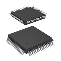
DF71251AD50FPV Renesas Electronics America, DF71251AD50FPV Datasheet - Page 318

DF71251AD50FPV
Manufacturer Part Number
DF71251AD50FPV
Description
MCU RISC FLASH 32K 8K 64LQFP
Manufacturer
Renesas Electronics America
Series
SuperH® SH Tinyr
Datasheet
1.DF71243N50FPV.pdf
(794 pages)
Specifications of DF71251AD50FPV
Core Processor
SH-2
Core Size
32-Bit
Speed
50MHz
Connectivity
SCI
Peripherals
POR, PWM, WDT
Number Of I /o
37
Program Memory Size
32KB (32K x 8)
Program Memory Type
FLASH
Ram Size
8K x 8
Voltage - Supply (vcc/vdd)
4 V ~ 5.5 V
Data Converters
A/D 8x10b
Oscillator Type
External
Operating Temperature
-40°C ~ 85°C
Package / Case
64-LQFP
Lead Free Status / RoHS Status
Lead free / RoHS Compliant
Eeprom Size
-
Available stocks
Company
Part Number
Manufacturer
Quantity
Price
Company:
Part Number:
DF71251AD50FPV
Manufacturer:
Renesas Electronics America
Quantity:
10 000
- Current page: 318 of 794
- Download datasheet (5Mb)
16. Example of AC Synchronous Motor (Brushless DC Motor) Drive Waveform Output
Rev. 5.00 Mar. 06, 2009 Page 298 of 770
REJ09B0243-0500
In complementary PWM mode, a brushless DC motor can easily be controlled using the timer
gate control register (TGCR). Figures 9.63 to 9.66 show examples of brushless DC motor drive
waveforms created using TGCR.
When output phase switching for a 3-phase brushless DC motor is performed by means of
external signals detected with a Hall element, etc., clear the FB bit in TGCR to 0. In this case,
the external signals indicating the polarity position are input to channel 0 timer input pins
TIOC0A, TIOC0B, and TIOC0C (set with PFC). When an edge is detected at pin TIOC0A,
TIOC0B, or TIOC0C, the output on/off state is switched automatically.
When the FB bit is 1, the output on/off state is switched when the UF, VF, or WF bit in TGCR
is cleared to 0 or set to 1.
The drive waveforms are output from the complementary PWM mode 6-phase output pins.
With this 6-phase output, in the case of on output, it is possible to use complementary PWM
mode output and perform chopping output by setting the N bit or P bit to 1. When the N bit or
P bit is 0, level output is selected.
The 6-phase output active level (on output level) can be set with the OLSN and OLSP bits in
the timer output control register (TOCR) regardless of the setting of the N and P bits.
Figure 9.63 Example of Output Phase Switching by External Input (1)
External input
6-phase output
When BDC = 1, N = 0, P = 0, FB = 0, output active level = high
TIOC0A pin
TIOC0B pin
TIOC0C pin
TIOC3B pin
TIOC3D pin
TIOC4A pin
TIOC4C pin
TIOC4B pin
TIOC4D pin
Related parts for DF71251AD50FPV
Image
Part Number
Description
Manufacturer
Datasheet
Request
R

Part Number:
Description:
KIT STARTER FOR M16C/29
Manufacturer:
Renesas Electronics America
Datasheet:

Part Number:
Description:
KIT STARTER FOR R8C/2D
Manufacturer:
Renesas Electronics America
Datasheet:

Part Number:
Description:
R0K33062P STARTER KIT
Manufacturer:
Renesas Electronics America
Datasheet:

Part Number:
Description:
KIT STARTER FOR R8C/23 E8A
Manufacturer:
Renesas Electronics America
Datasheet:

Part Number:
Description:
KIT STARTER FOR R8C/25
Manufacturer:
Renesas Electronics America
Datasheet:

Part Number:
Description:
KIT STARTER H8S2456 SHARPE DSPLY
Manufacturer:
Renesas Electronics America
Datasheet:

Part Number:
Description:
KIT STARTER FOR R8C38C
Manufacturer:
Renesas Electronics America
Datasheet:

Part Number:
Description:
KIT STARTER FOR R8C35C
Manufacturer:
Renesas Electronics America
Datasheet:

Part Number:
Description:
KIT STARTER FOR R8CL3AC+LCD APPS
Manufacturer:
Renesas Electronics America
Datasheet:

Part Number:
Description:
KIT STARTER FOR RX610
Manufacturer:
Renesas Electronics America
Datasheet:

Part Number:
Description:
KIT STARTER FOR R32C/118
Manufacturer:
Renesas Electronics America
Datasheet:

Part Number:
Description:
KIT DEV RSK-R8C/26-29
Manufacturer:
Renesas Electronics America
Datasheet:

Part Number:
Description:
KIT STARTER FOR SH7124
Manufacturer:
Renesas Electronics America
Datasheet:

Part Number:
Description:
KIT STARTER FOR H8SX/1622
Manufacturer:
Renesas Electronics America
Datasheet:

Part Number:
Description:
KIT DEV FOR SH7203
Manufacturer:
Renesas Electronics America
Datasheet:


