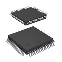
DF71251AD50FPV Renesas Electronics America, DF71251AD50FPV Datasheet - Page 485

DF71251AD50FPV
Manufacturer Part Number
DF71251AD50FPV
Description
MCU RISC FLASH 32K 8K 64LQFP
Manufacturer
Renesas Electronics America
Series
SuperH® SH Tinyr
Datasheet
1.DF71243N50FPV.pdf
(794 pages)
Specifications of DF71251AD50FPV
Core Processor
SH-2
Core Size
32-Bit
Speed
50MHz
Connectivity
SCI
Peripherals
POR, PWM, WDT
Number Of I /o
37
Program Memory Size
32KB (32K x 8)
Program Memory Type
FLASH
Ram Size
8K x 8
Voltage - Supply (vcc/vdd)
4 V ~ 5.5 V
Data Converters
A/D 8x10b
Oscillator Type
External
Operating Temperature
-40°C ~ 85°C
Package / Case
64-LQFP
Lead Free Status / RoHS Status
Lead free / RoHS Compliant
Eeprom Size
-
Available stocks
Company
Part Number
Manufacturer
Quantity
Price
Company:
Part Number:
DF71251AD50FPV
Manufacturer:
Renesas Electronics America
Quantity:
10 000
- Current page: 485 of 794
- Download datasheet (5Mb)
Section 12 Serial Communication Interface (SCI)
12.4.4
Multiprocessor Communication Function
Use of the multiprocessor communication function enables data transfer to be performed among a
number of processors sharing communication lines by means of asynchronous serial
communication using the multiprocessor format, in which a multiprocessor bit is added to the
transfer data. When multiprocessor communication is carried out, each receiving station is
addressed by a unique ID code. The serial communication cycle consists of two component cycles:
an ID transmission cycle that specifies the receiving station, and a data transmission cycle. The
multiprocessor bit is used to differentiate between the ID transmission cycle and the data
transmission cycle. If the multiprocessor bit is 1, the cycle is an ID transmission cycle, and if the
multiprocessor bit is 0, the cycle is a data transmission cycle. Figure 12.15 shows an example of
inter-processor communication using the multiprocessor format. The transmitting station first
sends the ID code of the receiving station with which it wants to perform serial communication as
data with a 1 multiprocessor bit added. It then sends transmit data as data with a 0 multiprocessor
bit added. The receiving station skips data until data with a 1 multiprocessor bit is sent. When data
with a 1 multiprocessor bit is received, the receiving station compares that data with its own ID.
The station whose ID matches then receives the data sent next. Stations whose ID does not match
continue to skip data until data with a 1 multiprocessor bit is again received.
The SCI uses the MPIE bit in SCSCR to implement this function. When the MPIE bit is set to 1,
transfer of receive data from SCRSR to SCRDR, error flag detection, and setting the SCSSR status
flags, RDRF, FER, and OER to 1 are inhibited until data with a 1 multiprocessor bit is received.
On reception of receive character with a 1 multiprocessor bit, the MPB bit in SCSSR is set to 1
and the MPIE bit is automatically cleared, thus normal reception is resumed. If the RIE bit in
SCSCR is set to 1 at this time, an RXI interrupt is generated.
When the multiprocessor format is selected, the parity bit setting is invalid. All other bit settings
are the same as those in normal asynchronous mode. The clock used for multiprocessor
communication is the same as that in normal asynchronous mode.
Rev. 5.00 Mar. 06, 2009 Page 465 of 770
REJ09B0243-0500
Related parts for DF71251AD50FPV
Image
Part Number
Description
Manufacturer
Datasheet
Request
R

Part Number:
Description:
KIT STARTER FOR M16C/29
Manufacturer:
Renesas Electronics America
Datasheet:

Part Number:
Description:
KIT STARTER FOR R8C/2D
Manufacturer:
Renesas Electronics America
Datasheet:

Part Number:
Description:
R0K33062P STARTER KIT
Manufacturer:
Renesas Electronics America
Datasheet:

Part Number:
Description:
KIT STARTER FOR R8C/23 E8A
Manufacturer:
Renesas Electronics America
Datasheet:

Part Number:
Description:
KIT STARTER FOR R8C/25
Manufacturer:
Renesas Electronics America
Datasheet:

Part Number:
Description:
KIT STARTER H8S2456 SHARPE DSPLY
Manufacturer:
Renesas Electronics America
Datasheet:

Part Number:
Description:
KIT STARTER FOR R8C38C
Manufacturer:
Renesas Electronics America
Datasheet:

Part Number:
Description:
KIT STARTER FOR R8C35C
Manufacturer:
Renesas Electronics America
Datasheet:

Part Number:
Description:
KIT STARTER FOR R8CL3AC+LCD APPS
Manufacturer:
Renesas Electronics America
Datasheet:

Part Number:
Description:
KIT STARTER FOR RX610
Manufacturer:
Renesas Electronics America
Datasheet:

Part Number:
Description:
KIT STARTER FOR R32C/118
Manufacturer:
Renesas Electronics America
Datasheet:

Part Number:
Description:
KIT DEV RSK-R8C/26-29
Manufacturer:
Renesas Electronics America
Datasheet:

Part Number:
Description:
KIT STARTER FOR SH7124
Manufacturer:
Renesas Electronics America
Datasheet:

Part Number:
Description:
KIT STARTER FOR H8SX/1622
Manufacturer:
Renesas Electronics America
Datasheet:

Part Number:
Description:
KIT DEV FOR SH7203
Manufacturer:
Renesas Electronics America
Datasheet:


