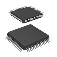
DF71251AD50FPV Renesas Electronics America, DF71251AD50FPV Datasheet - Page 162

DF71251AD50FPV
Manufacturer Part Number
DF71251AD50FPV
Description
MCU RISC FLASH 32K 8K 64LQFP
Manufacturer
Renesas Electronics America
Series
SuperH® SH Tinyr
Datasheet
1.DF71243N50FPV.pdf
(794 pages)
Specifications of DF71251AD50FPV
Core Processor
SH-2
Core Size
32-Bit
Speed
50MHz
Connectivity
SCI
Peripherals
POR, PWM, WDT
Number Of I /o
37
Program Memory Size
32KB (32K x 8)
Program Memory Type
FLASH
Ram Size
8K x 8
Voltage - Supply (vcc/vdd)
4 V ~ 5.5 V
Data Converters
A/D 8x10b
Oscillator Type
External
Operating Temperature
-40°C ~ 85°C
Package / Case
64-LQFP
Lead Free Status / RoHS Status
Lead free / RoHS Compliant
Eeprom Size
-
Available stocks
Company
Part Number
Manufacturer
Quantity
Price
Company:
Part Number:
DF71251AD50FPV
Manufacturer:
Renesas Electronics America
Quantity:
10 000
- Current page: 162 of 794
- Download datasheet (5Mb)
(Example 1-3)
• Register specifications
(Example 1-4)
• Register specifications
Rev. 5.00 Mar. 06, 2009 Page 142 of 770
REJ09B0243-0500
<Channel B>
Address:
Data:
Bus cycle: L bus/instruction fetch (before instruction execution)/read/word
After an instruction with address H'00037226 is executed, a user break occurs before an
instruction with address H'0003722E is executed.
BARA = H'00027128, BAMRA = H'00000000, BBRA = H'005A, BDRA = H'00000000,
BDMRA = H'00000000, BARB = H'00031415, BAMRB = H'00000000, BBRB = H'0054,
BDRB = H'00000000, BDMRB = H'00000000, BRCR = H'00000000
Specified conditions: Channel A/channel B independent mode
<Channel A>
Address:
Data:
Bus cycle: L bus/instruction fetch (before instruction execution)/write/word
<Channel B>
Address:
Data:
Bus cycle: L bus/instruction fetch (before instruction execution)/read (operand size is not
On channel A, no user break occurs since instruction fetch is not a write cycle. On channel B,
no user break occurs since instruction fetch is performed for an even address.
BARA = H'00037226, BAMRA = H'00000000, BBRA = H'005A, BDRA = H'00000000,
BDMRA = H'00000000, BARB = H'0003722E, BAMRB = H'00000000, BBRB = H'0056,
BDRB = H'00000000, BDMRB = H'00000000, BRCR = H'00000008
Specified conditions: Channel A/channel B sequential mode
<Channel A>
Address:
Data:
Bus cycle: L bus/instruction fetch (before instruction execution)/write/word
H'00000000, Data mask: H'00000000
H'00027128, Address mask: H'00000000
H'00000000, Data mask: H'00000000
H'00031415, Address mask: H'00000000
H'00000000, Data mask: H'00000000
included in the condition)
H'00037226, Address mask: H'00000000
H'00000000, Data mask: H'00000000
H'0003722E, Address mask: H'00000000
Related parts for DF71251AD50FPV
Image
Part Number
Description
Manufacturer
Datasheet
Request
R

Part Number:
Description:
KIT STARTER FOR M16C/29
Manufacturer:
Renesas Electronics America
Datasheet:

Part Number:
Description:
KIT STARTER FOR R8C/2D
Manufacturer:
Renesas Electronics America
Datasheet:

Part Number:
Description:
R0K33062P STARTER KIT
Manufacturer:
Renesas Electronics America
Datasheet:

Part Number:
Description:
KIT STARTER FOR R8C/23 E8A
Manufacturer:
Renesas Electronics America
Datasheet:

Part Number:
Description:
KIT STARTER FOR R8C/25
Manufacturer:
Renesas Electronics America
Datasheet:

Part Number:
Description:
KIT STARTER H8S2456 SHARPE DSPLY
Manufacturer:
Renesas Electronics America
Datasheet:

Part Number:
Description:
KIT STARTER FOR R8C38C
Manufacturer:
Renesas Electronics America
Datasheet:

Part Number:
Description:
KIT STARTER FOR R8C35C
Manufacturer:
Renesas Electronics America
Datasheet:

Part Number:
Description:
KIT STARTER FOR R8CL3AC+LCD APPS
Manufacturer:
Renesas Electronics America
Datasheet:

Part Number:
Description:
KIT STARTER FOR RX610
Manufacturer:
Renesas Electronics America
Datasheet:

Part Number:
Description:
KIT STARTER FOR R32C/118
Manufacturer:
Renesas Electronics America
Datasheet:

Part Number:
Description:
KIT DEV RSK-R8C/26-29
Manufacturer:
Renesas Electronics America
Datasheet:

Part Number:
Description:
KIT STARTER FOR SH7124
Manufacturer:
Renesas Electronics America
Datasheet:

Part Number:
Description:
KIT STARTER FOR H8SX/1622
Manufacturer:
Renesas Electronics America
Datasheet:

Part Number:
Description:
KIT DEV FOR SH7203
Manufacturer:
Renesas Electronics America
Datasheet:


