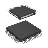
DF71251AD50FPV Renesas Electronics America, DF71251AD50FPV Datasheet - Page 633

DF71251AD50FPV
Manufacturer Part Number
DF71251AD50FPV
Description
MCU RISC FLASH 32K 8K 64LQFP
Manufacturer
Renesas Electronics America
Series
SuperH® SH Tinyr
Datasheet
1.DF71243N50FPV.pdf
(794 pages)
Specifications of DF71251AD50FPV
Core Processor
SH-2
Core Size
32-Bit
Speed
50MHz
Connectivity
SCI
Peripherals
POR, PWM, WDT
Number Of I /o
37
Program Memory Size
32KB (32K x 8)
Program Memory Type
FLASH
Ram Size
8K x 8
Voltage - Supply (vcc/vdd)
4 V ~ 5.5 V
Data Converters
A/D 8x10b
Oscillator Type
External
Operating Temperature
-40°C ~ 85°C
Package / Case
64-LQFP
Lead Free Status / RoHS Status
Lead free / RoHS Compliant
Eeprom Size
-
Available stocks
Company
Part Number
Manufacturer
Quantity
Price
Company:
Part Number:
DF71251AD50FPV
Manufacturer:
Renesas Electronics America
Quantity:
10 000
- Current page: 633 of 794
- Download datasheet (5Mb)
(2) State Transition Diagram
Note that the command for reading from the user MAT can only read data that has been
programmed after automatic erasure of the entire user MAT.
Figure 17.8 gives an overview of the state transitions after the chip has been started up in boot
mode. For details on boot mode, see section 17.8.1, Specifications of the Standard Serial
Communications Interface in Boot Mode.
1. Bit-rate matching
2. Waiting for inquiry and selection commands
3. Automatic erasure of the entire user MAT
4. Waiting for programming/erasure command
⎯ On receiving the programming selection command, the chip waits for data to be
⎯ On receiving the erasure select command, the chip waits for the block number of a block to
⎯ In addition to the programming and erasure commands, commands for sum checking and
After the chip has been started up in boot mode, bit-rate matching between the SCI and the
host proceeds.
The chip sends the requested information to the host in response to inquiries regarding the
size and configuration of the user MAT, start addresses of the MATs, information on
supported devices, etc.
After all necessary inquiries and selections have been made and the command for transition
to the programming/erasure state is sent by the host, the entire user MAT is automatically
erased.
programmed. To program data, the host transmits the programming command code
followed by the address where programming should start and the data to be programmed.
This is repeated as required while the chip is in the programming-selected state. To
terminate programming, H'FFFFFFFF should be transmitted as the first address of the area
for programming. This makes the chip return to the programming/erasure command
waiting state from the programming data waiting state.
be erased. To erase a block, the host transmits the erasure command code followed by the
number of the block to be erased. This is repeated as required while the chip is in the
erasure-selected state. To terminate erasure, H'FF should be transmitted as the block
number. This makes the chip return to the programming/erasure command waiting state
from the erasure block number waiting state. Erasure should only be executed when a
specific block is to be reprogrammed without executing a reset-start of the chip after the
flash memory has been programmed in boot mode. If all desired programming is done in a
single operation, such erasure processing is not necessary because all blocks are erased
before the chip enters the programming/erasure/other command waiting state.
blank checking (checking for erasure) of the user MAT, reading data from the user MAT,
and acquiring current state information are provided.
Rev. 5.00 Mar. 06, 2009 Page 613 of 770
REJ09B0243-0500
Related parts for DF71251AD50FPV
Image
Part Number
Description
Manufacturer
Datasheet
Request
R

Part Number:
Description:
KIT STARTER FOR M16C/29
Manufacturer:
Renesas Electronics America
Datasheet:

Part Number:
Description:
KIT STARTER FOR R8C/2D
Manufacturer:
Renesas Electronics America
Datasheet:

Part Number:
Description:
R0K33062P STARTER KIT
Manufacturer:
Renesas Electronics America
Datasheet:

Part Number:
Description:
KIT STARTER FOR R8C/23 E8A
Manufacturer:
Renesas Electronics America
Datasheet:

Part Number:
Description:
KIT STARTER FOR R8C/25
Manufacturer:
Renesas Electronics America
Datasheet:

Part Number:
Description:
KIT STARTER H8S2456 SHARPE DSPLY
Manufacturer:
Renesas Electronics America
Datasheet:

Part Number:
Description:
KIT STARTER FOR R8C38C
Manufacturer:
Renesas Electronics America
Datasheet:

Part Number:
Description:
KIT STARTER FOR R8C35C
Manufacturer:
Renesas Electronics America
Datasheet:

Part Number:
Description:
KIT STARTER FOR R8CL3AC+LCD APPS
Manufacturer:
Renesas Electronics America
Datasheet:

Part Number:
Description:
KIT STARTER FOR RX610
Manufacturer:
Renesas Electronics America
Datasheet:

Part Number:
Description:
KIT STARTER FOR R32C/118
Manufacturer:
Renesas Electronics America
Datasheet:

Part Number:
Description:
KIT DEV RSK-R8C/26-29
Manufacturer:
Renesas Electronics America
Datasheet:

Part Number:
Description:
KIT STARTER FOR SH7124
Manufacturer:
Renesas Electronics America
Datasheet:

Part Number:
Description:
KIT STARTER FOR H8SX/1622
Manufacturer:
Renesas Electronics America
Datasheet:

Part Number:
Description:
KIT DEV FOR SH7203
Manufacturer:
Renesas Electronics America
Datasheet:


