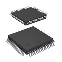
DF71251AD50FPV Renesas Electronics America, DF71251AD50FPV Datasheet - Page 82

DF71251AD50FPV
Manufacturer Part Number
DF71251AD50FPV
Description
MCU RISC FLASH 32K 8K 64LQFP
Manufacturer
Renesas Electronics America
Series
SuperH® SH Tinyr
Datasheet
1.DF71243N50FPV.pdf
(794 pages)
Specifications of DF71251AD50FPV
Core Processor
SH-2
Core Size
32-Bit
Speed
50MHz
Connectivity
SCI
Peripherals
POR, PWM, WDT
Number Of I /o
37
Program Memory Size
32KB (32K x 8)
Program Memory Type
FLASH
Ram Size
8K x 8
Voltage - Supply (vcc/vdd)
4 V ~ 5.5 V
Data Converters
A/D 8x10b
Oscillator Type
External
Operating Temperature
-40°C ~ 85°C
Package / Case
64-LQFP
Lead Free Status / RoHS Status
Lead free / RoHS Compliant
Eeprom Size
-
Available stocks
Company
Part Number
Manufacturer
Quantity
Price
Company:
Part Number:
DF71251AD50FPV
Manufacturer:
Renesas Electronics America
Quantity:
10 000
- Current page: 82 of 794
- Download datasheet (5Mb)
Table 4.4
Notes: * Clock frequencies when the input clock frequency is assumed to be the shown value.
Rev. 5.00 Mar. 06, 2009 Page 62 of 770
REJ09B0243-0500
PLL
Multipli-
cation
Ratio
×8
1. The PLL multiplication ratio is fixed at ×8. The division ratio can be selected from ×1/2,
2. The output frequency of the PLL circuit is the product of the frequency of the input from
3. The input to the divider is always the output from the PLL circuit.
4. The internal clock (Iφ) frequency is the product of the frequency of the input from the
5. The peripheral clock (Pφ) frequency is the product of the frequency of the input from the
6. When using the MTU2, the MTU2 clock (MPφ) frequency must be equal to or higher
7. The frequency of the CK pin is always be equal to the bus clock (Bφ) frequency.
8. The bus clock (Bφ) frequency must be equal to the peripheral clock (Pφ) frequency.
Iφ
1/8
1/4
1/4
1/2
1/2
1/8
1/4
1/4
1/2
The internal clock (Iφ) frequency must be 10 to 50 MHz and the peripheral clock (Pφ)
frequency must be 10 to 40 MHz. The bus clock (Bφ) frequency must be equal to the
peripheral clock (Pφ) frequency.
×1/4, and ×1/8 for each clock by the setting in the frequency control register.
the crystal resonator or EXTAL pin and the multiplication ratio (×8) of the PLL circuit.
crystal resonator or EXTAL pin, the multiplication ratio (×8) of the PLL circuit, and the
division ratio of the divider. The resultant frequency must be a maximum of 50 MHz
(maximum operating frequency).
crystal resonator or EXTAL pin, the multiplication ratio (×8) of the PLL circuit, and the
division ratio of the divider. The resultant frequency must be a maximum of 40 MHz.
than the peripheral clock frequency (Pφ). The MTU2 clock (MPφ) frequency are the
product of the frequency of the input from the crystal resonator or EXTAL pin, the
multiplication ratio (×8) of the PLL circuit, and the division ratio of the divider.
FRQCR Division Ratio
Frequency Division Ratios Specifiable with FRQCR
Bφ
1/8
1/8
1/4
1/4
1/2
1/8
1/8
1/4
1/4
Setting
Pφ
1/8
1/8
1/4
1/4
1/2
1/8
1/8
1/4
1/4
MPφ
1/8
1/8
1/4
1/4
1/2
1/8
1/8
1/4
1/4
Iφ
1
2
2
4
4
1
2
2
4
Bφ
1
1
2
2
4
1
1
2
2
Clock Ratio
Pφ
1
1
2
2
4
1
1
2
2
MPφ
1
1
2
2
4
1
1
2
2
Input
Clock
10
10
10
10
10
12.5
12.5
12.5
12.5
Clock Frequency (MHz)*
Iφ
10
20
20
40
40
12.5
25
25
50
Bφ
10
10
20
20
40
12.5
12.5
25
25
Pφ
10
10
20
20
40
12.5
12.5
25
25
MPφ
10
10
20
20
40
12.5
12.5
25
25
Related parts for DF71251AD50FPV
Image
Part Number
Description
Manufacturer
Datasheet
Request
R

Part Number:
Description:
KIT STARTER FOR M16C/29
Manufacturer:
Renesas Electronics America
Datasheet:

Part Number:
Description:
KIT STARTER FOR R8C/2D
Manufacturer:
Renesas Electronics America
Datasheet:

Part Number:
Description:
R0K33062P STARTER KIT
Manufacturer:
Renesas Electronics America
Datasheet:

Part Number:
Description:
KIT STARTER FOR R8C/23 E8A
Manufacturer:
Renesas Electronics America
Datasheet:

Part Number:
Description:
KIT STARTER FOR R8C/25
Manufacturer:
Renesas Electronics America
Datasheet:

Part Number:
Description:
KIT STARTER H8S2456 SHARPE DSPLY
Manufacturer:
Renesas Electronics America
Datasheet:

Part Number:
Description:
KIT STARTER FOR R8C38C
Manufacturer:
Renesas Electronics America
Datasheet:

Part Number:
Description:
KIT STARTER FOR R8C35C
Manufacturer:
Renesas Electronics America
Datasheet:

Part Number:
Description:
KIT STARTER FOR R8CL3AC+LCD APPS
Manufacturer:
Renesas Electronics America
Datasheet:

Part Number:
Description:
KIT STARTER FOR RX610
Manufacturer:
Renesas Electronics America
Datasheet:

Part Number:
Description:
KIT STARTER FOR R32C/118
Manufacturer:
Renesas Electronics America
Datasheet:

Part Number:
Description:
KIT DEV RSK-R8C/26-29
Manufacturer:
Renesas Electronics America
Datasheet:

Part Number:
Description:
KIT STARTER FOR SH7124
Manufacturer:
Renesas Electronics America
Datasheet:

Part Number:
Description:
KIT STARTER FOR H8SX/1622
Manufacturer:
Renesas Electronics America
Datasheet:

Part Number:
Description:
KIT DEV FOR SH7203
Manufacturer:
Renesas Electronics America
Datasheet:


