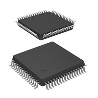
DF71251AD50FPV Renesas Electronics America, DF71251AD50FPV Datasheet - Page 640

DF71251AD50FPV
Manufacturer Part Number
DF71251AD50FPV
Description
MCU RISC FLASH 32K 8K 64LQFP
Manufacturer
Renesas Electronics America
Series
SuperH® SH Tinyr
Datasheet
1.DF71243N50FPV.pdf
(794 pages)
Specifications of DF71251AD50FPV
Core Processor
SH-2
Core Size
32-Bit
Speed
50MHz
Connectivity
SCI
Peripherals
POR, PWM, WDT
Number Of I /o
37
Program Memory Size
32KB (32K x 8)
Program Memory Type
FLASH
Ram Size
8K x 8
Voltage - Supply (vcc/vdd)
4 V ~ 5.5 V
Data Converters
A/D 8x10b
Oscillator Type
External
Operating Temperature
-40°C ~ 85°C
Package / Case
64-LQFP
Lead Free Status / RoHS Status
Lead free / RoHS Compliant
Eeprom Size
-
Available stocks
Company
Part Number
Manufacturer
Quantity
Price
Company:
Part Number:
DF71251AD50FPV
Manufacturer:
Renesas Electronics America
Quantity:
10 000
- Current page: 640 of 794
- Download datasheet (5Mb)
(2.7) Initialization
(2.8) The return value of the initialization program, FPFR (general register R0) is checked.
(2.9) FKEY must be set to H'5A and the user MAT must be prepared for programming.
(2.10) The parameter which is required for programming is set.
Rev. 5.00 Mar. 06, 2009 Page 620 of 770
REJ09B0243-0500
MOV.L #DLTOP+32,R1
JSR
NOP
When a programming program is downloaded, the initialization program is also downloaded to
on-chip RAM. There is an entry point of the initialization program in the area from (download
start address set by FTDAR) + 32 bytes. The subroutine is called and initialization is executed
by using the following steps.
The start address of the programming destination of the user MAT (FMPAR) is set to general
register R5. The start address of the program data storage area (FMPDR) is set to general
register R4.
• The start address in the user branch destination is set to the FUBRA parameter (general
• The general registers other than R0 are saved in the initialization program.
• R0 is a return value of the FPFR parameter.
• Since the stack area is used in the initialization program, a stack area of maximum 128
• Interrupts can be accepted during the execution of the initialization program. However,
• FMPAR setting
register R5).
When the user branch processing is not required, 0 must be set to FUBRA.
When the user branch is executed, the branch destination is executed in flash memory
other than the one that is to be programmed. The area of the on-chip program that is
downloaded cannot be set.
The program processing must be returned from the user branch processing by the RTS
instruction.
See the description in section 17.4.3 (2.2), Flash user branch address setting parameter
(FUBRA: general register R5 of CPU).
bytes must be reserved in RAM.
the program storage area and stack area in on-chip RAM and register values must not
be destroyed.
FMPAR specifies the programming destination start address. When an address other
than one in the user MAT area is specified, even if the programming program is
executed, programming is not executed and an error is returned to the return value
@R1
; Set entry address to R1
; Call initialization routine
Related parts for DF71251AD50FPV
Image
Part Number
Description
Manufacturer
Datasheet
Request
R

Part Number:
Description:
KIT STARTER FOR M16C/29
Manufacturer:
Renesas Electronics America
Datasheet:

Part Number:
Description:
KIT STARTER FOR R8C/2D
Manufacturer:
Renesas Electronics America
Datasheet:

Part Number:
Description:
R0K33062P STARTER KIT
Manufacturer:
Renesas Electronics America
Datasheet:

Part Number:
Description:
KIT STARTER FOR R8C/23 E8A
Manufacturer:
Renesas Electronics America
Datasheet:

Part Number:
Description:
KIT STARTER FOR R8C/25
Manufacturer:
Renesas Electronics America
Datasheet:

Part Number:
Description:
KIT STARTER H8S2456 SHARPE DSPLY
Manufacturer:
Renesas Electronics America
Datasheet:

Part Number:
Description:
KIT STARTER FOR R8C38C
Manufacturer:
Renesas Electronics America
Datasheet:

Part Number:
Description:
KIT STARTER FOR R8C35C
Manufacturer:
Renesas Electronics America
Datasheet:

Part Number:
Description:
KIT STARTER FOR R8CL3AC+LCD APPS
Manufacturer:
Renesas Electronics America
Datasheet:

Part Number:
Description:
KIT STARTER FOR RX610
Manufacturer:
Renesas Electronics America
Datasheet:

Part Number:
Description:
KIT STARTER FOR R32C/118
Manufacturer:
Renesas Electronics America
Datasheet:

Part Number:
Description:
KIT DEV RSK-R8C/26-29
Manufacturer:
Renesas Electronics America
Datasheet:

Part Number:
Description:
KIT STARTER FOR SH7124
Manufacturer:
Renesas Electronics America
Datasheet:

Part Number:
Description:
KIT STARTER FOR H8SX/1622
Manufacturer:
Renesas Electronics America
Datasheet:

Part Number:
Description:
KIT DEV FOR SH7203
Manufacturer:
Renesas Electronics America
Datasheet:


