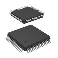
DF71251AD50FPV Renesas Electronics America, DF71251AD50FPV Datasheet - Page 599

DF71251AD50FPV
Manufacturer Part Number
DF71251AD50FPV
Description
MCU RISC FLASH 32K 8K 64LQFP
Manufacturer
Renesas Electronics America
Series
SuperH® SH Tinyr
Datasheet
1.DF71243N50FPV.pdf
(794 pages)
Specifications of DF71251AD50FPV
Core Processor
SH-2
Core Size
32-Bit
Speed
50MHz
Connectivity
SCI
Peripherals
POR, PWM, WDT
Number Of I /o
37
Program Memory Size
32KB (32K x 8)
Program Memory Type
FLASH
Ram Size
8K x 8
Voltage - Supply (vcc/vdd)
4 V ~ 5.5 V
Data Converters
A/D 8x10b
Oscillator Type
External
Operating Temperature
-40°C ~ 85°C
Package / Case
64-LQFP
Lead Free Status / RoHS Status
Lead free / RoHS Compliant
Eeprom Size
-
Available stocks
Company
Part Number
Manufacturer
Quantity
Price
Company:
Part Number:
DF71251AD50FPV
Manufacturer:
Renesas Electronics America
Quantity:
10 000
- Current page: 599 of 794
- Download datasheet (5Mb)
This LSI has 128-Kbyte, 64-Kbyte, 32-Kbyte, or 16-Kbyte on-chip flash memory. The flash
memory has the following features.
17.1
• Capacitance
• Two on-board programming modes and one off-board programming mode
• Programming/erasing interface by the download of on-chip program
• Protection modes
SH71253, SH71243: 128 Kbytes
SH71252, SH71242: 64 Kbytes
SH71251A. SH71241A: 32 Kbytes
SH71250A. SH71240A: 16 Kbytes
⎯ On-board programming modes
Boot Mode: This mode is a program mode that uses an on-chip SCI interface. The user MAT
can be programmed. This mode can automatically adjust the bit rate between the host and this
LSI.
User Program Mode: The user MAT can be programmed by using an interface selected by
the user. This mode cannot be used on the 32 Kbyte and 16 Kbyte flash memory versions.
⎯ Off-board programming mode
This mode uses the dedicated socket adapter and PROM programmer. The user MAT can be
programmed.
This LSI has a dedicated programming/erasing program. After downloading this program to
the on-chip RAM, programming/erasing can be performed by setting the argument parameter.
The user branch is also supported.
⎯ User branch
The program processing is performed in 128-byte units. It consists the program pulse
application, verify read, and several other steps. Erasing is performed in one divided-block
units and consists of several steps. The user processing routine can be executed between the
steps, this setting for which is called the user branch addition.
There are two protection modes. Software protection by the register setting and hardware
protection by the FWE pin. The protection state for flash memory programming/erasing can be
set.
When abnormalities, such as runaway of programming/erasing are detected, these modes enter
the error protection state and the programming/erasing processing is suspended.
Features
Section 17 Flash Memory (ROM)
Rev. 5.00 Mar. 06, 2009 Page 579 of 770
REJ09B0243-0500
Related parts for DF71251AD50FPV
Image
Part Number
Description
Manufacturer
Datasheet
Request
R

Part Number:
Description:
KIT STARTER FOR M16C/29
Manufacturer:
Renesas Electronics America
Datasheet:

Part Number:
Description:
KIT STARTER FOR R8C/2D
Manufacturer:
Renesas Electronics America
Datasheet:

Part Number:
Description:
R0K33062P STARTER KIT
Manufacturer:
Renesas Electronics America
Datasheet:

Part Number:
Description:
KIT STARTER FOR R8C/23 E8A
Manufacturer:
Renesas Electronics America
Datasheet:

Part Number:
Description:
KIT STARTER FOR R8C/25
Manufacturer:
Renesas Electronics America
Datasheet:

Part Number:
Description:
KIT STARTER H8S2456 SHARPE DSPLY
Manufacturer:
Renesas Electronics America
Datasheet:

Part Number:
Description:
KIT STARTER FOR R8C38C
Manufacturer:
Renesas Electronics America
Datasheet:

Part Number:
Description:
KIT STARTER FOR R8C35C
Manufacturer:
Renesas Electronics America
Datasheet:

Part Number:
Description:
KIT STARTER FOR R8CL3AC+LCD APPS
Manufacturer:
Renesas Electronics America
Datasheet:

Part Number:
Description:
KIT STARTER FOR RX610
Manufacturer:
Renesas Electronics America
Datasheet:

Part Number:
Description:
KIT STARTER FOR R32C/118
Manufacturer:
Renesas Electronics America
Datasheet:

Part Number:
Description:
KIT DEV RSK-R8C/26-29
Manufacturer:
Renesas Electronics America
Datasheet:

Part Number:
Description:
KIT STARTER FOR SH7124
Manufacturer:
Renesas Electronics America
Datasheet:

Part Number:
Description:
KIT STARTER FOR H8SX/1622
Manufacturer:
Renesas Electronics America
Datasheet:

Part Number:
Description:
KIT DEV FOR SH7203
Manufacturer:
Renesas Electronics America
Datasheet:


