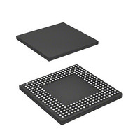
HD6417720BP133BV Renesas Electronics America, HD6417720BP133BV Datasheet - Page 1294

HD6417720BP133BV
Manufacturer Part Number
HD6417720BP133BV
Description
SH3-DSP, WITH USB AND LCDC, PB-F
Manufacturer
Renesas Electronics America
Series
SuperH® SH7700r
Datasheet
1.R8A77210C133BAV.pdf
(1478 pages)
Specifications of HD6417720BP133BV
Core Processor
SH-3 DSP
Core Size
32-Bit
Speed
133MHz
Connectivity
FIFO, I²C, IrDA, MMC, SCI, SD, SIO, SIM, USB
Peripherals
DMA, LCD, POR, WDT
Number Of I /o
117
Program Memory Type
ROMless
Ram Size
16K x 8
Voltage - Supply (vcc/vdd)
1.4 V ~ 1.6 V
Data Converters
A/D 4x10b; D/A 2x8b
Oscillator Type
Internal
Operating Temperature
-20°C ~ 75°C
Package / Case
256-BGA
Lead Free Status / RoHS Status
Lead free / RoHS Compliant
Eeprom Size
-
Program Memory Size
-
- Current page: 1294 of 1478
- Download datasheet (10Mb)
Section 36 User Debugging Interface (H-UDI)
36.5
A command can be set in SDIR by the H-UDI to place the H-UDI pins in the boundary scan mode
stipulated by JTAG.
36.5.1
This LSI supports the three essential instructions defined in the JTAG standard (BYPASS,
SAMPLE/PRELOAD, and EXTEST) and three option instructions (IDCODE, CLAMP, and
HIGHZ).
(1)
The BYPASS instruction is an essential standard instruction that operates the bypass register. This
instruction shortens the shift path to speed up serial data transfer involving other chips on the
printed circuit board. While this instruction is executing, the test circuit has no effect on the
system circuits. The upper four bits of the instruction code are B'1111.
(2)
The SAMPLE/PRELOAD instruction inputs values from this LSI's internal circuitry to the
boundary scan register, outputs values from the scan path, and loads data onto the scan path. When
this instruction is executing, this LSI's input pin signals are transmitted directly to the internal
circuitry, and internal circuit values are directly output externally from the output pins. This LSI's
system circuits are not affected by execution of this instruction. The upper four bits of the
instruction code are B'0100.
In a SAMPLE operation, a snapshot of a value to be transferred from an input pin to the internal
circuitry, or a value to be transferred from the internal circuitry to an output pin, is latched into the
boundary scan register and read from the scan path. Snapshot latching is performed in
synchronization with the rise of TCK in the Capture-DR state. Snapshot latching does not affect
normal operation of this LSI.
In a PRELOAD operation, an initial value is set in the parallel output latch of the boundary scan
register from the scan path prior to the EXTEST instruction. Without a PRELOAD operation,
when the EXTEST instruction was executed an undefined value would be output from the output
pin until completion of the initial scan sequence (transfer to the output latch) (with the EXTEST
instruction, the parallel output latch value is constantly output to the output pin).
Page 1234 of 1414
BYPASS
SAMPLE/PRELOAD
Supported Instructions
Boundary Scan
SH7720 Group, SH7721 Group
R01UH0083EJ0400 Rev. 4.00
Sep 21, 2010
Related parts for HD6417720BP133BV
Image
Part Number
Description
Manufacturer
Datasheet
Request
R

Part Number:
Description:
KIT STARTER FOR M16C/29
Manufacturer:
Renesas Electronics America
Datasheet:

Part Number:
Description:
KIT STARTER FOR R8C/2D
Manufacturer:
Renesas Electronics America
Datasheet:

Part Number:
Description:
R0K33062P STARTER KIT
Manufacturer:
Renesas Electronics America
Datasheet:

Part Number:
Description:
KIT STARTER FOR R8C/23 E8A
Manufacturer:
Renesas Electronics America
Datasheet:

Part Number:
Description:
KIT STARTER FOR R8C/25
Manufacturer:
Renesas Electronics America
Datasheet:

Part Number:
Description:
KIT STARTER H8S2456 SHARPE DSPLY
Manufacturer:
Renesas Electronics America
Datasheet:

Part Number:
Description:
KIT STARTER FOR R8C38C
Manufacturer:
Renesas Electronics America
Datasheet:

Part Number:
Description:
KIT STARTER FOR R8C35C
Manufacturer:
Renesas Electronics America
Datasheet:

Part Number:
Description:
KIT STARTER FOR R8CL3AC+LCD APPS
Manufacturer:
Renesas Electronics America
Datasheet:

Part Number:
Description:
KIT STARTER FOR RX610
Manufacturer:
Renesas Electronics America
Datasheet:

Part Number:
Description:
KIT STARTER FOR R32C/118
Manufacturer:
Renesas Electronics America
Datasheet:

Part Number:
Description:
KIT DEV RSK-R8C/26-29
Manufacturer:
Renesas Electronics America
Datasheet:

Part Number:
Description:
KIT STARTER FOR SH7124
Manufacturer:
Renesas Electronics America
Datasheet:

Part Number:
Description:
KIT STARTER FOR H8SX/1622
Manufacturer:
Renesas Electronics America
Datasheet:

Part Number:
Description:
KIT DEV FOR SH7203
Manufacturer:
Renesas Electronics America
Datasheet:


