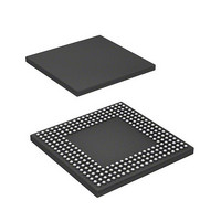
HD6417720BP133BV Renesas Electronics America, HD6417720BP133BV Datasheet - Page 488

HD6417720BP133BV
Manufacturer Part Number
HD6417720BP133BV
Description
SH3-DSP, WITH USB AND LCDC, PB-F
Manufacturer
Renesas Electronics America
Series
SuperH® SH7700r
Datasheet
1.R8A77210C133BAV.pdf
(1478 pages)
Specifications of HD6417720BP133BV
Core Processor
SH-3 DSP
Core Size
32-Bit
Speed
133MHz
Connectivity
FIFO, I²C, IrDA, MMC, SCI, SD, SIO, SIM, USB
Peripherals
DMA, LCD, POR, WDT
Number Of I /o
117
Program Memory Type
ROMless
Ram Size
16K x 8
Voltage - Supply (vcc/vdd)
1.4 V ~ 1.6 V
Data Converters
A/D 4x10b; D/A 2x8b
Oscillator Type
Internal
Operating Temperature
-20°C ~ 75°C
Package / Case
256-BGA
Lead Free Status / RoHS Status
Lead free / RoHS Compliant
Eeprom Size
-
Program Memory Size
-
- Current page: 488 of 1478
- Download datasheet (10Mb)
SH7720 Group, SH7721 Group
Section 10 Direct Memory Access Controller (DMAC)
(3)
On-Chip Peripheral Module Request Mode
In this mode, a transfer is performed at the transfer request signal of an on-chip peripheral module.
Transfer request signals comprise the transmit data empty transfer request and receive data full
transfer request from the ADC set by CHCR0 to CHCR5 and the SCIF0, SCIF1, MMC, USBF,
SIM, SIOF0, SIOF1, and SDHI set by DMARS0/1/2, and the compare-match timer transfer
request from the CMT (channels 0 to 4).
When this mode is selected, if the DMA transfer is enabled (DE = 1, DME = 1, TE = 0, AE = 0,
NMIF = 0), a transfer is performed upon the input of a transfer request signal.
When a transmit data empty transfer request of the SCIF0 is set as the transfer request, the transfer
destination must be the SCIF0's transmit data register. Likewise, when receive data full transfer
request of the SCIF0 is set as the transfer request, the transfer source must be the SCIF0's receive
data register. These conditions also apply to the SIOF1, MMC, USBF, SIM, SIOF0, SIOF1, and
SDHI. When the ADC is set as the transfer request, the transfer source must be the A/D data
register. Any address can be specified for data source and destination, when transfer request is
generated by the CMT (channels 0 to 4).
The number of the receive FIFO triggers can be set as a transfer request depending on an on-chip
peripheral module. Data needs to be read after the DMA transfer is ended, because data may be
remained in the receive FIFO when the receive FIFO trigger condition is not satisfied.
Page 428 of 1414
R01UH0083EJ0400 Rev. 4.00
Sep 21, 2010
Related parts for HD6417720BP133BV
Image
Part Number
Description
Manufacturer
Datasheet
Request
R

Part Number:
Description:
KIT STARTER FOR M16C/29
Manufacturer:
Renesas Electronics America
Datasheet:

Part Number:
Description:
KIT STARTER FOR R8C/2D
Manufacturer:
Renesas Electronics America
Datasheet:

Part Number:
Description:
R0K33062P STARTER KIT
Manufacturer:
Renesas Electronics America
Datasheet:

Part Number:
Description:
KIT STARTER FOR R8C/23 E8A
Manufacturer:
Renesas Electronics America
Datasheet:

Part Number:
Description:
KIT STARTER FOR R8C/25
Manufacturer:
Renesas Electronics America
Datasheet:

Part Number:
Description:
KIT STARTER H8S2456 SHARPE DSPLY
Manufacturer:
Renesas Electronics America
Datasheet:

Part Number:
Description:
KIT STARTER FOR R8C38C
Manufacturer:
Renesas Electronics America
Datasheet:

Part Number:
Description:
KIT STARTER FOR R8C35C
Manufacturer:
Renesas Electronics America
Datasheet:

Part Number:
Description:
KIT STARTER FOR R8CL3AC+LCD APPS
Manufacturer:
Renesas Electronics America
Datasheet:

Part Number:
Description:
KIT STARTER FOR RX610
Manufacturer:
Renesas Electronics America
Datasheet:

Part Number:
Description:
KIT STARTER FOR R32C/118
Manufacturer:
Renesas Electronics America
Datasheet:

Part Number:
Description:
KIT DEV RSK-R8C/26-29
Manufacturer:
Renesas Electronics America
Datasheet:

Part Number:
Description:
KIT STARTER FOR SH7124
Manufacturer:
Renesas Electronics America
Datasheet:

Part Number:
Description:
KIT STARTER FOR H8SX/1622
Manufacturer:
Renesas Electronics America
Datasheet:

Part Number:
Description:
KIT DEV FOR SH7203
Manufacturer:
Renesas Electronics America
Datasheet:


