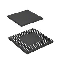
HD6417712BPV Renesas Electronics America, HD6417712BPV Datasheet - Page 139

HD6417712BPV
Manufacturer Part Number
HD6417712BPV
Description
MPU 1.5/3.3V 0K PB-FREE 256-BGA
Manufacturer
Renesas Electronics America
Series
SuperH® SH Ethernetr
Datasheet
1.HD6417712BPV.pdf
(980 pages)
Specifications of HD6417712BPV
Core Processor
SH-3 DSP
Core Size
32-Bit
Speed
200MHz
Connectivity
EBI/EMI, Ethernet, FIFO, SCI, SIO
Peripherals
DMA, POR, WDT
Number Of I /o
24
Program Memory Type
ROMless
Ram Size
16K x 8
Voltage - Supply (vcc/vdd)
1.4 V ~ 1.6 V
Oscillator Type
External
Operating Temperature
-20°C ~ 75°C
Package / Case
256-BGA
Lead Free Status / RoHS Status
Lead free / RoHS Compliant
Eeprom Size
-
Program Memory Size
-
Data Converters
-
Available stocks
Company
Part Number
Manufacturer
Quantity
Price
Company:
Part Number:
HD6417712BPV
Manufacturer:
Renesas Electronics America
Quantity:
10 000
- Current page: 139 of 980
- Download datasheet (6Mb)
Double data transfer instructions can be described in parallel to the DSP operation instructions.
Even if a conditional operation instruction is specified in parallel to a double data transfer
instruction, the specified condition does not affect the data transfer operations. For details, refer to
section 3.5, DSP Data Operation Instructions.
Double data transfer instructions can access only the X memory or Y memory and cannot access
other memory space. The X bus and Y bus are 16 bits and support 64-byte address spaces
corresponding to address areas H'A5000000 to H'A500FFFF and H'A5010000 to H'A501FFFF,
respectively. Because these areas are included in the P2/Uxy area, they are not affected by the
cache and address translation unit.
Single Data Transfer Instructions: The single data transfer instructions access any memory
location. All DSP registers other than the DSR* can be specified as source and destination
operands. Guard bit registers A0G and A1G can also be specified as two independent registers.
Because these instructions use the L bus (LAB and LDB), these instructions can access any logical
space handled by the CPU. If these instructions access the cacheable area while the cache is
enabled, the area accessed by these instructions are cached. The X memory and Y memory are
mapped to the logical address space and can also be accessed by the single data transfer
instructions. In this case, bus conflict may occur between data transfer and instruction fetch
because the CPU also uses the L bus for instruction fetches.
The single data transfer instructions can handle both word and longword data. In word data
transfer, only the upper word of the operand register is valid. In word data load, word data is
loaded into the upper word of the destination registers and the lower word of the destination is
automatically cleared to 0. If the guard bits are supported, the sign bit is extended before storage.
In longword data load, longword data is loaded into the upper and lower word of the destination
register. If the guard bits are supported, the sign bit is extended before storage. When the guard
register is stored, the sign bit is extended to the upper 24 bits of the LDB and are loaded onto the
LDB bus.
Notes: * Because the DSR register is defined as the system register, it can be accessed by the
System Control Instructions: The DSR, A0, X0, X1, Y0, and Y1 registers in the DSP unit can
also be used as the CPU system registers. Accordingly, data transfer operations between these
DSP system registers and general registers or memory can be executed by the STS and LDS
instructions. These DSP system registers can be treated as the CPU system register such as PR,
MACL and MACH and can use the same addressing modes.
1. Any data transfer instruction is executed at the MA stage of the pipeline.
2. Any data transfer instruction does not modify the condition code bits of the DSR
LDS or STS instruction.
register.
Rev. 1.00 Dec. 27, 2005 Page 95 of 1044
Section 3 DSP Operating Unit
REJ09B0269-0100
Related parts for HD6417712BPV
Image
Part Number
Description
Manufacturer
Datasheet
Request
R

Part Number:
Description:
KIT STARTER FOR M16C/29
Manufacturer:
Renesas Electronics America
Datasheet:

Part Number:
Description:
KIT STARTER FOR R8C/2D
Manufacturer:
Renesas Electronics America
Datasheet:

Part Number:
Description:
R0K33062P STARTER KIT
Manufacturer:
Renesas Electronics America
Datasheet:

Part Number:
Description:
KIT STARTER FOR R8C/23 E8A
Manufacturer:
Renesas Electronics America
Datasheet:

Part Number:
Description:
KIT STARTER FOR R8C/25
Manufacturer:
Renesas Electronics America
Datasheet:

Part Number:
Description:
KIT STARTER H8S2456 SHARPE DSPLY
Manufacturer:
Renesas Electronics America
Datasheet:

Part Number:
Description:
KIT STARTER FOR R8C38C
Manufacturer:
Renesas Electronics America
Datasheet:

Part Number:
Description:
KIT STARTER FOR R8C35C
Manufacturer:
Renesas Electronics America
Datasheet:

Part Number:
Description:
KIT STARTER FOR R8CL3AC+LCD APPS
Manufacturer:
Renesas Electronics America
Datasheet:

Part Number:
Description:
KIT STARTER FOR RX610
Manufacturer:
Renesas Electronics America
Datasheet:

Part Number:
Description:
KIT STARTER FOR R32C/118
Manufacturer:
Renesas Electronics America
Datasheet:

Part Number:
Description:
KIT DEV RSK-R8C/26-29
Manufacturer:
Renesas Electronics America
Datasheet:

Part Number:
Description:
KIT STARTER FOR SH7124
Manufacturer:
Renesas Electronics America
Datasheet:

Part Number:
Description:
KIT STARTER FOR H8SX/1622
Manufacturer:
Renesas Electronics America
Datasheet:

Part Number:
Description:
KIT DEV FOR SH7203
Manufacturer:
Renesas Electronics America
Datasheet:


