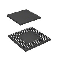
HD6417712BPV Renesas Electronics America, HD6417712BPV Datasheet - Page 836

HD6417712BPV
Manufacturer Part Number
HD6417712BPV
Description
MPU 1.5/3.3V 0K PB-FREE 256-BGA
Manufacturer
Renesas Electronics America
Series
SuperH® SH Ethernetr
Datasheet
1.HD6417712BPV.pdf
(980 pages)
Specifications of HD6417712BPV
Core Processor
SH-3 DSP
Core Size
32-Bit
Speed
200MHz
Connectivity
EBI/EMI, Ethernet, FIFO, SCI, SIO
Peripherals
DMA, POR, WDT
Number Of I /o
24
Program Memory Type
ROMless
Ram Size
16K x 8
Voltage - Supply (vcc/vdd)
1.4 V ~ 1.6 V
Oscillator Type
External
Operating Temperature
-20°C ~ 75°C
Package / Case
256-BGA
Lead Free Status / RoHS Status
Lead free / RoHS Compliant
Eeprom Size
-
Program Memory Size
-
Data Converters
-
Available stocks
Company
Part Number
Manufacturer
Quantity
Price
Company:
Part Number:
HD6417712BPV
Manufacturer:
Renesas Electronics America
Quantity:
10 000
- Current page: 836 of 980
- Download datasheet (6Mb)
Section 22 User Debugging Interface (H-UDI)
22.2
Table 22.1 shows the pin configuration of the H-UDI.
Table 22.1 Pin Configuration
Rev. 1.00 Dec. 27, 2005 Page 792 of 932
REJ09B0269-0100
Pin Name
TCK
TMS
TRST
TDI
TDO
ASEMD0
Input/Output Pins
Input/Output
Input
Input
Input
Input
Output
Input
Description
Serial Data Input/Output Clock Pin
Data is serially supplied to the H-UDI from the data input pin
(TDI), and output from the data output pin (TDO), in
synchronization with this clock.
Mode Select Input Pin
The state of the TAP control circuit is determined by changing
this signal in synchronization with TCK. The protocol conforms
to the JTAG standard (IEEE Std.1149.1).
Reset Input Pin
Input is accepted asynchronously with respect to TCK, and
when low, the H-UDI is reset. TRST must be low for a constant
period when power is turned on regardless of using the H-UDI
function. As the same as the RESETP pin, the TRST pin should
be driven low at the power-on reset state and driven high after
the power-on reset state is released. This is different from the
JTAG standard.
See section 22.4.2, Reset Configuration, for more information.
Serial Data Input Pin
Data transfer to the H-UDI is executed by changing this signal
in synchronization with TCK.
Serial Data Output Pin
Data read from the H-UDI is executed by reading this pin in
synchronization with TCK. The data output timing depends on
the command type set in the SDIR. See section 22.4.3 TDO
Output Timing, for more information.
ASE Mode Select Pin
If a low level is input at the ASEMD0 pin while the RESETP pin
is asserted, ASE mode is entered; if a high level is input,
normal mode is entered. In ASE mode, dedicated emulator
function can be used. The input level at the ASEMD0 pin
should be held for at least one cycle after RESETP negation.
Related parts for HD6417712BPV
Image
Part Number
Description
Manufacturer
Datasheet
Request
R

Part Number:
Description:
KIT STARTER FOR M16C/29
Manufacturer:
Renesas Electronics America
Datasheet:

Part Number:
Description:
KIT STARTER FOR R8C/2D
Manufacturer:
Renesas Electronics America
Datasheet:

Part Number:
Description:
R0K33062P STARTER KIT
Manufacturer:
Renesas Electronics America
Datasheet:

Part Number:
Description:
KIT STARTER FOR R8C/23 E8A
Manufacturer:
Renesas Electronics America
Datasheet:

Part Number:
Description:
KIT STARTER FOR R8C/25
Manufacturer:
Renesas Electronics America
Datasheet:

Part Number:
Description:
KIT STARTER H8S2456 SHARPE DSPLY
Manufacturer:
Renesas Electronics America
Datasheet:

Part Number:
Description:
KIT STARTER FOR R8C38C
Manufacturer:
Renesas Electronics America
Datasheet:

Part Number:
Description:
KIT STARTER FOR R8C35C
Manufacturer:
Renesas Electronics America
Datasheet:

Part Number:
Description:
KIT STARTER FOR R8CL3AC+LCD APPS
Manufacturer:
Renesas Electronics America
Datasheet:

Part Number:
Description:
KIT STARTER FOR RX610
Manufacturer:
Renesas Electronics America
Datasheet:

Part Number:
Description:
KIT STARTER FOR R32C/118
Manufacturer:
Renesas Electronics America
Datasheet:

Part Number:
Description:
KIT DEV RSK-R8C/26-29
Manufacturer:
Renesas Electronics America
Datasheet:

Part Number:
Description:
KIT STARTER FOR SH7124
Manufacturer:
Renesas Electronics America
Datasheet:

Part Number:
Description:
KIT STARTER FOR H8SX/1622
Manufacturer:
Renesas Electronics America
Datasheet:

Part Number:
Description:
KIT DEV FOR SH7203
Manufacturer:
Renesas Electronics America
Datasheet:


