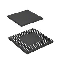
HD6417712BPV Renesas Electronics America, HD6417712BPV Datasheet - Page 35

HD6417712BPV
Manufacturer Part Number
HD6417712BPV
Description
MPU 1.5/3.3V 0K PB-FREE 256-BGA
Manufacturer
Renesas Electronics America
Series
SuperH® SH Ethernetr
Datasheet
1.HD6417712BPV.pdf
(980 pages)
Specifications of HD6417712BPV
Core Processor
SH-3 DSP
Core Size
32-Bit
Speed
200MHz
Connectivity
EBI/EMI, Ethernet, FIFO, SCI, SIO
Peripherals
DMA, POR, WDT
Number Of I /o
24
Program Memory Type
ROMless
Ram Size
16K x 8
Voltage - Supply (vcc/vdd)
1.4 V ~ 1.6 V
Oscillator Type
External
Operating Temperature
-20°C ~ 75°C
Package / Case
256-BGA
Lead Free Status / RoHS Status
Lead free / RoHS Compliant
Eeprom Size
-
Program Memory Size
-
Data Converters
-
Available stocks
Company
Part Number
Manufacturer
Quantity
Price
Company:
Part Number:
HD6417712BPV
Manufacturer:
Renesas Electronics America
Quantity:
10 000
- Current page: 35 of 980
- Download datasheet (6Mb)
Figure 18.7 (2) MII Frame Transmit Timing (Collision)............................................................ 717
Figure 18.7 (3) MII Frame Transmit Timing (Transmit Error)................................................... 718
Figure 18.7 (4) MII Frame Receive Timing (Normal Reception)............................................... 718
Figure 18.7 (5) MII Frame Receive Timing (Reception Error (1))............................................. 718
Figure 18.7 (6) MII Fame Receive Timing (Reception Error (2)) .............................................. 718
Figure 18.8 MII Management Frame Format ............................................................................. 719
Figure 18.9 (1) 1-Bit Data Write Flowchart ............................................................................... 720
Figure 18.9 (2) Bus Release Flowchart (TA in Read in Figure 18.8) ......................................... 721
Figure 18.9 (3) 1-Bit Data Read Flowchart ................................................................................ 721
Figure 18.9 (4) Independent Bus Release Flowchart (IDLE in Write in Figure 18.8)................ 722
Figure 18.10 Changing IPG and Transmission Efficiency ......................................................... 723
Figure 18.11 Diagram of Qtag Additional Functions ................................................................. 724
Figure 18.12 Comparison of Normal Ethernet Frame and IEEE802.1Q Frame (with Qtag)...... 724
Figure 18.13 Example of Connection to DP83847 ..................................................................... 725
Section 19 Ethernet Controller Direct Memory Access Controller (E-DMAC)
Figure 19.1 Configuration of E-DMAC, and Descriptors and Buffers....................................... 728
Figure 19.2 Relationship between Transmit Descriptor and Transmit Buffer ............................ 755
Figure 19.3 Relationship between Receive Descriptor and Receive Buffer ............................... 761
Figure 19.4 Sample Transmission
................................ 768
Flowchart (Single-Frame/Two-Descriptor)
Figure 19.5 Sample Reception Flowchart (Single-Frame/Two-Descriptor) ............................... 770
Figure 19.6 E-DMAC Operation after Transmit Error ............................................................... 771
Figure 19.7 E-DMAC Operation after Receive Error................................................................. 772
Figure 19.8 Configuration of ARBUSY ..................................................................................... 773
Figure 19.9 Summary of Receive FIFO Overflow Alert Signal ................................................. 774
Figure 19.10 ARBUSY Signal Change and Minimum Pulse Width Depending on
Increase and Decrease of FIFO ............................................................................. 775
Section 22 User Debugging Interface (H-UDI)
Figure 22.1 Block Diagram of H-UDI........................................................................................ 791
Figure 22.2 TAP Controller State Transitions ............................................................................ 802
Figure 22.3 H-UDI Data Transfer Timing.................................................................................. 804
Figure 22.4 H-UDI Reset............................................................................................................ 804
Section 24 Electrical Characteristics
Figure 24.1 Power On/Off Sequence .......................................................................................... 856
Figure 24.2 EXTAL Clock Input Timing ................................................................................... 861
Figure 24.3 CKIO Clock Input Timing....................................................................................... 861
Figure 24.4 CKIO Clock Output Timing.................................................................................... 862
Figure 24.5 Power-On Oscillation Settling Time ....................................................................... 862
Figure 24.6 Oscillation Settling Time at Standby Return (Return by Reset).............................. 862
Figure 24.7 Oscillation Settling Time at Standby Return (Return by NMI)............................... 863
Rev. 1.00 Dec. 27, 2005 Page xxxiii of xlii
Related parts for HD6417712BPV
Image
Part Number
Description
Manufacturer
Datasheet
Request
R

Part Number:
Description:
KIT STARTER FOR M16C/29
Manufacturer:
Renesas Electronics America
Datasheet:

Part Number:
Description:
KIT STARTER FOR R8C/2D
Manufacturer:
Renesas Electronics America
Datasheet:

Part Number:
Description:
R0K33062P STARTER KIT
Manufacturer:
Renesas Electronics America
Datasheet:

Part Number:
Description:
KIT STARTER FOR R8C/23 E8A
Manufacturer:
Renesas Electronics America
Datasheet:

Part Number:
Description:
KIT STARTER FOR R8C/25
Manufacturer:
Renesas Electronics America
Datasheet:

Part Number:
Description:
KIT STARTER H8S2456 SHARPE DSPLY
Manufacturer:
Renesas Electronics America
Datasheet:

Part Number:
Description:
KIT STARTER FOR R8C38C
Manufacturer:
Renesas Electronics America
Datasheet:

Part Number:
Description:
KIT STARTER FOR R8C35C
Manufacturer:
Renesas Electronics America
Datasheet:

Part Number:
Description:
KIT STARTER FOR R8CL3AC+LCD APPS
Manufacturer:
Renesas Electronics America
Datasheet:

Part Number:
Description:
KIT STARTER FOR RX610
Manufacturer:
Renesas Electronics America
Datasheet:

Part Number:
Description:
KIT STARTER FOR R32C/118
Manufacturer:
Renesas Electronics America
Datasheet:

Part Number:
Description:
KIT DEV RSK-R8C/26-29
Manufacturer:
Renesas Electronics America
Datasheet:

Part Number:
Description:
KIT STARTER FOR SH7124
Manufacturer:
Renesas Electronics America
Datasheet:

Part Number:
Description:
KIT STARTER FOR H8SX/1622
Manufacturer:
Renesas Electronics America
Datasheet:

Part Number:
Description:
KIT DEV FOR SH7203
Manufacturer:
Renesas Electronics America
Datasheet:


