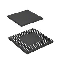
HD6417712BPV Renesas Electronics America, HD6417712BPV Datasheet - Page 34

HD6417712BPV
Manufacturer Part Number
HD6417712BPV
Description
MPU 1.5/3.3V 0K PB-FREE 256-BGA
Manufacturer
Renesas Electronics America
Series
SuperH® SH Ethernetr
Datasheet
1.HD6417712BPV.pdf
(980 pages)
Specifications of HD6417712BPV
Core Processor
SH-3 DSP
Core Size
32-Bit
Speed
200MHz
Connectivity
EBI/EMI, Ethernet, FIFO, SCI, SIO
Peripherals
DMA, POR, WDT
Number Of I /o
24
Program Memory Type
ROMless
Ram Size
16K x 8
Voltage - Supply (vcc/vdd)
1.4 V ~ 1.6 V
Oscillator Type
External
Operating Temperature
-20°C ~ 75°C
Package / Case
256-BGA
Lead Free Status / RoHS Status
Lead free / RoHS Compliant
Eeprom Size
-
Program Memory Size
-
Data Converters
-
Available stocks
Company
Part Number
Manufacturer
Quantity
Price
Company:
Part Number:
HD6417712BPV
Manufacturer:
Renesas Electronics America
Quantity:
10 000
- Current page: 34 of 980
- Download datasheet (6Mb)
Figure 16.10 RTS Control Operation ......................................................................................... 572
Figure 16.11 Data Format in Clock Synchronous Communication............................................ 572
Figure 16.12 Sample the SCIF Initialization Flowchart ............................................................. 574
Figure 16.13 Sample Serial Transmission Flowchart ................................................................. 575
Figure 16.14 Example of the SCIF Transmit Operation............................................................. 576
Figure 16.15 Sample Serial Reception Flowchart ...................................................................... 577
Figure 16.16 Sample Serial Reception Flowchart ...................................................................... 578
Figure 16.17 Example of the SCIF Receive Operation .............................................................. 579
Figure 16.18 Sample Serial Data Transmission/Reception Flowchart ....................................... 581
Figure 16.19 Receive Data Sampling Timing in Asynchronous Mode ...................................... 584
Figure 16.20 Sample Transfer of Synchronous Clock by DMAC .............................................. 585
Section 17 Serial I/O with FIFO (SIOF)
Figure 17.1 Block Diagram of SIOF .......................................................................................... 588
Figure 17.2 Serial Clock Supply................................................................................................. 613
Figure 17.3 Serial Data Synchronization Timing ....................................................................... 615
Figure 17.4 SIOF Transmit/Receive Timing .............................................................................. 616
Figure 17.5 Transmit/Receive Data Bit Alignment .................................................................... 618
Figure 17.6 Control Data Bit Alignment .................................................................................... 619
Figure 17.7 Control Data Interface (Slot Position)..................................................................... 620
Figure 17.8 Control Data Interface (Secondary FS) ................................................................... 621
Figure 17.9 Example of Transmission Operation in Master Mode............................................. 624
Figure 17.10 Example of Reception Operation in Master Mode ................................................ 625
Figure 17.11 Example of Transmission Operation in Slave Mode............................................. 626
Figure 17.12 Example of Reception Operation in Slave Mode .................................................. 627
Figure 17.13 Transmission and Reception Timings (8-Bit Monaural Data (1)) ......................... 631
Figure 17.14 Transmission and Reception Timings (8-Bit Monaural Data (2)) ......................... 631
Figure 17.15 Transmission and Reception Timings (16-Bit Monaural Data (1)) ....................... 632
Figure 17.16 Transmission and Reception Timings (16-Bit Stereo Data (1)) ............................ 632
Figure 17.17 Transmission and Reception Timings (16-Bit Stereo Data (2)) ............................ 633
Figure 17.18 Transmission and Reception Timings (16-Bit Stereo Data (3)) ............................ 633
Figure 17.19 Transmission and Reception Timings (16-Bit Monaural Data (2)) ....................... 634
Section 18 Ethernet Controller (EtherC)
Figure 18.1 Configuration of EtherC.......................................................................................... 638
Figure 18.2 EtherC Data Path and Various Settings................................................................... 707
Figure 18.3 EtherC Transmitter State Transitions ...................................................................... 708
Figure 18.4 EtherC Receiver State Transmissions ..................................................................... 710
Figure 18.5 Example of External CAM Connection .................................................................. 714
Figure 18.6 External CAM Signal Timing ................................................................................. 716
Figure 18.7 (1) MII Frame Transmit Timing (Normal Transmission)........................................ 717
Rev. 1.00 Dec. 27, 2005 Page xxxii of xlii
Related parts for HD6417712BPV
Image
Part Number
Description
Manufacturer
Datasheet
Request
R

Part Number:
Description:
KIT STARTER FOR M16C/29
Manufacturer:
Renesas Electronics America
Datasheet:

Part Number:
Description:
KIT STARTER FOR R8C/2D
Manufacturer:
Renesas Electronics America
Datasheet:

Part Number:
Description:
R0K33062P STARTER KIT
Manufacturer:
Renesas Electronics America
Datasheet:

Part Number:
Description:
KIT STARTER FOR R8C/23 E8A
Manufacturer:
Renesas Electronics America
Datasheet:

Part Number:
Description:
KIT STARTER FOR R8C/25
Manufacturer:
Renesas Electronics America
Datasheet:

Part Number:
Description:
KIT STARTER H8S2456 SHARPE DSPLY
Manufacturer:
Renesas Electronics America
Datasheet:

Part Number:
Description:
KIT STARTER FOR R8C38C
Manufacturer:
Renesas Electronics America
Datasheet:

Part Number:
Description:
KIT STARTER FOR R8C35C
Manufacturer:
Renesas Electronics America
Datasheet:

Part Number:
Description:
KIT STARTER FOR R8CL3AC+LCD APPS
Manufacturer:
Renesas Electronics America
Datasheet:

Part Number:
Description:
KIT STARTER FOR RX610
Manufacturer:
Renesas Electronics America
Datasheet:

Part Number:
Description:
KIT STARTER FOR R32C/118
Manufacturer:
Renesas Electronics America
Datasheet:

Part Number:
Description:
KIT DEV RSK-R8C/26-29
Manufacturer:
Renesas Electronics America
Datasheet:

Part Number:
Description:
KIT STARTER FOR SH7124
Manufacturer:
Renesas Electronics America
Datasheet:

Part Number:
Description:
KIT STARTER FOR H8SX/1622
Manufacturer:
Renesas Electronics America
Datasheet:

Part Number:
Description:
KIT DEV FOR SH7203
Manufacturer:
Renesas Electronics America
Datasheet:


