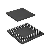
HD6417712BPV Renesas Electronics America, HD6417712BPV Datasheet - Page 32

HD6417712BPV
Manufacturer Part Number
HD6417712BPV
Description
MPU 1.5/3.3V 0K PB-FREE 256-BGA
Manufacturer
Renesas Electronics America
Series
SuperH® SH Ethernetr
Datasheet
1.HD6417712BPV.pdf
(980 pages)
Specifications of HD6417712BPV
Core Processor
SH-3 DSP
Core Size
32-Bit
Speed
200MHz
Connectivity
EBI/EMI, Ethernet, FIFO, SCI, SIO
Peripherals
DMA, POR, WDT
Number Of I /o
24
Program Memory Type
ROMless
Ram Size
16K x 8
Voltage - Supply (vcc/vdd)
1.4 V ~ 1.6 V
Oscillator Type
External
Operating Temperature
-20°C ~ 75°C
Package / Case
256-BGA
Lead Free Status / RoHS Status
Lead free / RoHS Compliant
Eeprom Size
-
Program Memory Size
-
Data Converters
-
Available stocks
Company
Part Number
Manufacturer
Quantity
Price
Company:
Part Number:
HD6417712BPV
Manufacturer:
Renesas Electronics America
Quantity:
10 000
- Current page: 32 of 980
- Download datasheet (6Mb)
Figure 12.26 Self-Refresh Timing .............................................................................................. 432
Figure 12.27 Access Timing in Low-Frequency Mode .............................................................. 433
Figure 12.28 Access Timing in Power-Down Mode .................................................................. 434
Figure 12.29 Write Timing for SDRAM Mode Register (Based on JEDEC)............................. 437
Figure 12.30 EMRS Command Issue Timing............................................................................. 439
Figure 12.31 Transition Timing in Deep Power-Down Mode.................................................... 440
Figure 12.32 Burst ROM (Clock Asynchronous) Access (Bus Width = 32 Bits,
Figure 12.33 Basic Access Timing for Byte-Selection SRAM (BAS = 0) ................................. 443
Figure 12.34 Basic Access Timing for Byte-Selection SRAM (BAS = 1) ................................. 444
Figure 12.35 Wait Timing for Byte-Selection SRAM (BAS = 1) (Software Wait Only)........... 445
Figure 12.36 Example of Connection with 32-Bit Data-Width Byte-Selection SRAM ............. 446
Figure 12.37 Example of Connection with 16-Bit Data-Width Byte-Selection SRAM ............. 446
Figure 12.38 Example of PCMCIA Interface Connection.......................................................... 448
Figure 12.39 Basic Access Timing for PCMCIA Memory Card Interface................................. 449
Figure 12.40 Wait Timing for PCMCIA Memory Card Interface (TED[3:0] = B′0010,
Figure 12.41 Example of PCMCIA Space Assignment (CS5BWCR.SA[1:0] = B′10,
Figure 12.42 Basic Timing for PCMCIA I/O Card Interface ..................................................... 451
Figure 12.43 Wait Timing for PCMCIA I/O Card Interface (TED[3:0] = B′0010,
Figure 12.44 Timing for Dynamic Bus Sizing of PCMCIA I/O Card Interface
Figure 12.45 Burst ROM (Clock Synchronous) Access Timing (Burst Length = 8,
Figure 12.46 Bus Arbitration Timing ......................................................................................... 456
Section 13 Direct Memory Access Controller (DMAC)
Figure 13.1 Block Diagram of DMAC ....................................................................................... 460
Figure 13.2 DMA Transfer Flowchart........................................................................................ 476
Figure 13.3 Round-Robin Mode................................................................................................. 480
Figure 13.4 Changes in Channel Priority in Round-Robin Mode............................................... 481
Figure 13.5 Data Flow in Dual Address Mode ........................................................................... 483
Figure 13.6 Example of DMA Transfer Timing in Dual Address Mode
Figure 13.7 Data Flow in Single Address Mode......................................................................... 485
Figure 13.8 Example of DMA Transfer Timing in Single Address Mode ................................. 486
Rev. 1.00 Dec. 27, 2005 Page xxx of xlii
(Source: Ordinary memory, Destination: Ordinary memory) ................................. 484
16-byte Transfer (Number of Bursts = 4), Access Wait for First Time = 2,
Access Wait for 2nd Time and after = 1).............................................................. 442
TEH[3:0] = B′0001, Software Wait = 1, Hardware Wait = 1) .............................. 449
CS6BWCR.SA[1:0] = B′10)................................................................................. 450
TEH[3:0] = B′0001, Software Wait = 1, Hardware Wait = 1) .............................. 452
(TED[3:0] = B′0010, TEH[3:0] = B′0001, Software Waits = 3) .......................... 452
Wait Cycles inserted in First Access = 2, Wait Cycles inserted in Second and
Subsequent Accesses = 1)..................................................................................... 453
Related parts for HD6417712BPV
Image
Part Number
Description
Manufacturer
Datasheet
Request
R

Part Number:
Description:
KIT STARTER FOR M16C/29
Manufacturer:
Renesas Electronics America
Datasheet:

Part Number:
Description:
KIT STARTER FOR R8C/2D
Manufacturer:
Renesas Electronics America
Datasheet:

Part Number:
Description:
R0K33062P STARTER KIT
Manufacturer:
Renesas Electronics America
Datasheet:

Part Number:
Description:
KIT STARTER FOR R8C/23 E8A
Manufacturer:
Renesas Electronics America
Datasheet:

Part Number:
Description:
KIT STARTER FOR R8C/25
Manufacturer:
Renesas Electronics America
Datasheet:

Part Number:
Description:
KIT STARTER H8S2456 SHARPE DSPLY
Manufacturer:
Renesas Electronics America
Datasheet:

Part Number:
Description:
KIT STARTER FOR R8C38C
Manufacturer:
Renesas Electronics America
Datasheet:

Part Number:
Description:
KIT STARTER FOR R8C35C
Manufacturer:
Renesas Electronics America
Datasheet:

Part Number:
Description:
KIT STARTER FOR R8CL3AC+LCD APPS
Manufacturer:
Renesas Electronics America
Datasheet:

Part Number:
Description:
KIT STARTER FOR RX610
Manufacturer:
Renesas Electronics America
Datasheet:

Part Number:
Description:
KIT STARTER FOR R32C/118
Manufacturer:
Renesas Electronics America
Datasheet:

Part Number:
Description:
KIT DEV RSK-R8C/26-29
Manufacturer:
Renesas Electronics America
Datasheet:

Part Number:
Description:
KIT STARTER FOR SH7124
Manufacturer:
Renesas Electronics America
Datasheet:

Part Number:
Description:
KIT STARTER FOR H8SX/1622
Manufacturer:
Renesas Electronics America
Datasheet:

Part Number:
Description:
KIT DEV FOR SH7203
Manufacturer:
Renesas Electronics America
Datasheet:


