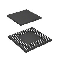
HD6417712BPV Renesas Electronics America, HD6417712BPV Datasheet - Page 37

HD6417712BPV
Manufacturer Part Number
HD6417712BPV
Description
MPU 1.5/3.3V 0K PB-FREE 256-BGA
Manufacturer
Renesas Electronics America
Series
SuperH® SH Ethernetr
Datasheet
1.HD6417712BPV.pdf
(980 pages)
Specifications of HD6417712BPV
Core Processor
SH-3 DSP
Core Size
32-Bit
Speed
200MHz
Connectivity
EBI/EMI, Ethernet, FIFO, SCI, SIO
Peripherals
DMA, POR, WDT
Number Of I /o
24
Program Memory Type
ROMless
Ram Size
16K x 8
Voltage - Supply (vcc/vdd)
1.4 V ~ 1.6 V
Oscillator Type
External
Operating Temperature
-20°C ~ 75°C
Package / Case
256-BGA
Lead Free Status / RoHS Status
Lead free / RoHS Compliant
Eeprom Size
-
Program Memory Size
-
Data Converters
-
Available stocks
Company
Part Number
Manufacturer
Quantity
Price
Company:
Part Number:
HD6417712BPV
Manufacturer:
Renesas Electronics America
Quantity:
10 000
- Current page: 37 of 980
- Download datasheet (6Mb)
Figure 24.32 Synchronous DRAM Burst Read Bus Cycle (Single Read × 4)
Figure 24.33 Synchronous DRAM Burst Write Bus Cycle (Single Write × 4)
Figure 24.34 Synchronous DRAM Burst Write Bus Cycle (Single Write × 4)
Figure 24.35 Synchronous DRAM Burst Write Bus Cycle (Single Write × 4)
Figure 24.36 Synchronous DRAM Auto-Refresh Timing (TRP = 2 Cycle) .............................. 889
Figure 24.37 Synchronous DRAM Self-Refresh Timing (TRP = 2 Cycle) ................................ 890
Figure 24.38 Synchronous DRAM Mode Register Write Timing (TRP = 2 Cycle)................... 891
Figure 24.39 PCMCIA Memory Card Interface Bus Timing ..................................................... 892
Figure 24.40 PCMCIA Memory Card Interface Bus Timing (TED[3:0] = B'0010,
Figure 24.41 PCMCIA I/O Card Interface Bus Timing.............................................................. 894
Figure 24.42 PCMCIA I/O Card Interface Bus Timing (TED[3:0] = B'0010,
Figure 24.43 REFOUT Delay Time ........................................................................................... 895
Figure 24.44 Access Timing in Low-Frequency Mode (Auto Precharge).................................. 897
Figure 24.45 Synchronous DRAM Auto-Refresh Timing (TRP = 2 Cycle,
Figure 24.46 Synchronous DRAM Self-Refresh Timing (TRP = 2 Cycle,
Figure 24.47 Synchronous DRAM Mode Register Write Timing (TRP = 2 Cycle,
Figure 24.48 DREQn Input Timing ............................................................................................ 901
Figure 24.49 TENDn, DACKn Output Timing .......................................................................... 901
Figure 24.50 Oscillation Settling Time when RTC Crystal Oscillator is Turned On ................. 902
Figure 24.51 SCIFnCK Input Clock Timing .............................................................................. 903
Figure 24.52 SCIF Input/Output Timing in Clock Synchronous Mode...................................... 904
Figure 24.53 SIOMCLK Input Timing....................................................................................... 905
Figure 24.54 SIOF Transmit/Receive Timing (Master Mode 1: Fall Sampling Time)............... 905
Figure 24.55 SIOF Transmit/Receive Timing (Master Mode 1: Rise Sampling Time).............. 906
Figure 24.56 SIOF Transmit/Receive Timing (Master Mode 2: Fall Sampling Time)............... 906
Figure 24.57 SIOF Transmit/Receive Timing (Master Mode 2: Rise Sampling Time).............. 907
Figure 24.58 SIOF Transmit/Receive Timing (Slave Mode 1 and Slave Mode 2)..................... 907
(Bank Active Mode, PRE + ACTV + READ Commands, Different
Row Address, CAS Latency = 2, TRCD = 1 Cycle)............................................. 885
(Bank Active Mode, ACTV + WRITE Commands, TRCD = 1 Cycle,
TRWL = 1 Cycle) ................................................................................................. 886
(Bank Active Mode, WRITE Command, Same Row Address,
TRCD = 1 Cycle, TRWL = 1 Cycle) .................................................................... 887
(Bank Active Mode, PRE + ACTV + WRITE Commands,
Different Row Address, TRCD = 1 Cycle, TRWL = 1 Cycle) ............................. 888
TEH[3:0] = B'0001, One Software Wait, One Hardware Wait)............................ 893
TEH[3:0] = B'0001, One Software Wait, One Hardware Wait)............................ 895
Low-Frequency Mode) ......................................................................................... 898
Low-Frequency Mode) ......................................................................................... 899
Low-Frequency Mode) ......................................................................................... 900
Rev. 1.00 Dec. 27, 2005 Page xxxv of xlii
Related parts for HD6417712BPV
Image
Part Number
Description
Manufacturer
Datasheet
Request
R

Part Number:
Description:
KIT STARTER FOR M16C/29
Manufacturer:
Renesas Electronics America
Datasheet:

Part Number:
Description:
KIT STARTER FOR R8C/2D
Manufacturer:
Renesas Electronics America
Datasheet:

Part Number:
Description:
R0K33062P STARTER KIT
Manufacturer:
Renesas Electronics America
Datasheet:

Part Number:
Description:
KIT STARTER FOR R8C/23 E8A
Manufacturer:
Renesas Electronics America
Datasheet:

Part Number:
Description:
KIT STARTER FOR R8C/25
Manufacturer:
Renesas Electronics America
Datasheet:

Part Number:
Description:
KIT STARTER H8S2456 SHARPE DSPLY
Manufacturer:
Renesas Electronics America
Datasheet:

Part Number:
Description:
KIT STARTER FOR R8C38C
Manufacturer:
Renesas Electronics America
Datasheet:

Part Number:
Description:
KIT STARTER FOR R8C35C
Manufacturer:
Renesas Electronics America
Datasheet:

Part Number:
Description:
KIT STARTER FOR R8CL3AC+LCD APPS
Manufacturer:
Renesas Electronics America
Datasheet:

Part Number:
Description:
KIT STARTER FOR RX610
Manufacturer:
Renesas Electronics America
Datasheet:

Part Number:
Description:
KIT STARTER FOR R32C/118
Manufacturer:
Renesas Electronics America
Datasheet:

Part Number:
Description:
KIT DEV RSK-R8C/26-29
Manufacturer:
Renesas Electronics America
Datasheet:

Part Number:
Description:
KIT STARTER FOR SH7124
Manufacturer:
Renesas Electronics America
Datasheet:

Part Number:
Description:
KIT STARTER FOR H8SX/1622
Manufacturer:
Renesas Electronics America
Datasheet:

Part Number:
Description:
KIT DEV FOR SH7203
Manufacturer:
Renesas Electronics America
Datasheet:


