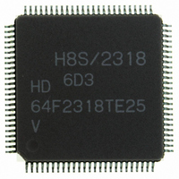
HD64F2318VTE25 Renesas Electronics America, HD64F2318VTE25 Datasheet - Page 544

HD64F2318VTE25
Manufacturer Part Number
HD64F2318VTE25
Description
IC H8S MCU FLASH 256K 100-QFP
Manufacturer
Renesas Electronics America
Series
H8® H8S/2300r
Specifications of HD64F2318VTE25
Core Processor
H8S/2000
Core Size
16-Bit
Speed
25MHz
Connectivity
SCI, SmartCard
Peripherals
POR, PWM, WDT
Number Of I /o
71
Program Memory Size
256KB (256K x 8)
Program Memory Type
FLASH
Ram Size
8K x 8
Voltage - Supply (vcc/vdd)
2.7 V ~ 3.6 V
Data Converters
A/D 8x10b; D/A 2x8b
Oscillator Type
Internal
Operating Temperature
-20°C ~ 75°C
Package / Case
100-TQFP, 100-VQFP
Lead Free Status / RoHS Status
Contains lead / RoHS non-compliant
Eeprom Size
-
- Current page: 544 of 1146
- Download datasheet (7Mb)
Section 13 Smart Card Interface
13.3.2
Figure 13.2 shows a schematic diagram of smart card interface related pin connections.
In communication with an IC card, since both transmission and reception are carried out on a
single data communication line, the chip’s TxD pin and RxD pin should both be connected to the
line, as shown in the figure. The data communication line should be pulled up to the V
supply with a resistor.
When the clock generated on the smart card interface is used by an IC card, the SCK pin output is
input to the CLK pin of the IC card. No connection is needed if the IC card uses an internal clock.
Chip port output is used as the reset signal.
Other pins must normally be connected to the power supply or ground.
Note: If an IC card is not connected, and the TE and RE bits are both set to 1, closed
Rev.7.00 Feb. 14, 2007 page 510 of 1108
REJ09B0089-0700
transmission/reception is possible, enabling self-diagnosis to be carried out.
Figure 13.2 Schematic Diagram of Smart Card Interface Pin Connections
Pin Connections
Chip
Connected equipment
Rx (port)
SCK
RxD
TxD
Data line
Clock line
Reset line
V
CC
I/O
CLK
RST
IC card
CC
power
Related parts for HD64F2318VTE25
Image
Part Number
Description
Manufacturer
Datasheet
Request
R

Part Number:
Description:
KIT STARTER FOR M16C/29
Manufacturer:
Renesas Electronics America
Datasheet:

Part Number:
Description:
KIT STARTER FOR R8C/2D
Manufacturer:
Renesas Electronics America
Datasheet:

Part Number:
Description:
R0K33062P STARTER KIT
Manufacturer:
Renesas Electronics America
Datasheet:

Part Number:
Description:
KIT STARTER FOR R8C/23 E8A
Manufacturer:
Renesas Electronics America
Datasheet:

Part Number:
Description:
KIT STARTER FOR R8C/25
Manufacturer:
Renesas Electronics America
Datasheet:

Part Number:
Description:
KIT STARTER H8S2456 SHARPE DSPLY
Manufacturer:
Renesas Electronics America
Datasheet:

Part Number:
Description:
KIT STARTER FOR R8C38C
Manufacturer:
Renesas Electronics America
Datasheet:

Part Number:
Description:
KIT STARTER FOR R8C35C
Manufacturer:
Renesas Electronics America
Datasheet:

Part Number:
Description:
KIT STARTER FOR R8CL3AC+LCD APPS
Manufacturer:
Renesas Electronics America
Datasheet:

Part Number:
Description:
KIT STARTER FOR RX610
Manufacturer:
Renesas Electronics America
Datasheet:

Part Number:
Description:
KIT STARTER FOR R32C/118
Manufacturer:
Renesas Electronics America
Datasheet:

Part Number:
Description:
KIT DEV RSK-R8C/26-29
Manufacturer:
Renesas Electronics America
Datasheet:

Part Number:
Description:
KIT STARTER FOR SH7124
Manufacturer:
Renesas Electronics America
Datasheet:

Part Number:
Description:
KIT STARTER FOR H8SX/1622
Manufacturer:
Renesas Electronics America
Datasheet:

Part Number:
Description:
KIT DEV FOR SH7203
Manufacturer:
Renesas Electronics America
Datasheet:


