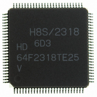
HD64F2318VTE25 Renesas Electronics America, HD64F2318VTE25 Datasheet - Page 637

HD64F2318VTE25
Manufacturer Part Number
HD64F2318VTE25
Description
IC H8S MCU FLASH 256K 100-QFP
Manufacturer
Renesas Electronics America
Series
H8® H8S/2300r
Specifications of HD64F2318VTE25
Core Processor
H8S/2000
Core Size
16-Bit
Speed
25MHz
Connectivity
SCI, SmartCard
Peripherals
POR, PWM, WDT
Number Of I /o
71
Program Memory Size
256KB (256K x 8)
Program Memory Type
FLASH
Ram Size
8K x 8
Voltage - Supply (vcc/vdd)
2.7 V ~ 3.6 V
Data Converters
A/D 8x10b; D/A 2x8b
Oscillator Type
Internal
Operating Temperature
-20°C ~ 75°C
Package / Case
100-TQFP, 100-VQFP
Lead Free Status / RoHS Status
Contains lead / RoHS non-compliant
Eeprom Size
-
- Current page: 637 of 1146
- Download datasheet (7Mb)
Table 17.12 Software Protection
Item
SWE bit protection
Block specification
protection
Emulation protection •
17.8.3
In error protection, an error is detected when MCU runaway occurs during flash memory
programming/erasing, or operation is not performed in accordance with the program/erase
algorithm, and the program/erase operation is aborted. Aborting the program/erase operation
prevents damage to the flash memory due to overprogramming or overerasing.
If the MCU malfunctions during flash memory programming/erasing, the FLER bit is set to 1 in
FLMCR2 and the error protection state is entered. The FLMCR1, FLMCR2, EBR1, and EBR2
settings are retained, but program mode or erase mode is aborted at the point at which the error
occurred. Program mode or erase mode cannot be re-entered by re-setting the P or E bit. However,
PV and EV bit setting is enabled, and a transition can be made to verify mode.
FLER bit setting conditions are as follows:
• When flash memory is read during programming/erasing (including a vector read or instruction
• Immediately after exception handling (excluding a reset) during programming/erasing
• When a SLEEP instruction (including software standby) is executed during
fetch)
programming/erasing
Error Protection
Description
•
•
•
Clearing the SWE bit to 0 in FLMCR1 sets
the program/erase-protected state for all
blocks
(Execute in on-chip RAM or external
memory.)
Erase protection can be set for individual
blocks by settings in erase block registers 1
and 2 (EBR1, EBR2).
Setting EBR1 and EBR2 to H'00 places all
blocks in the erase-protected state.
Setting the RAMS bit to 1 in the RAM
emulation register (RAMER) places all blocks
in the program/erase-protected state.
Rev.7.00 Feb. 14, 2007 page 603 of 1108
Program
Yes
—
Yes
Functions
REJ09B0089-0700
Section 17 ROM
Erase
Yes
Yes
Yes
Related parts for HD64F2318VTE25
Image
Part Number
Description
Manufacturer
Datasheet
Request
R

Part Number:
Description:
KIT STARTER FOR M16C/29
Manufacturer:
Renesas Electronics America
Datasheet:

Part Number:
Description:
KIT STARTER FOR R8C/2D
Manufacturer:
Renesas Electronics America
Datasheet:

Part Number:
Description:
R0K33062P STARTER KIT
Manufacturer:
Renesas Electronics America
Datasheet:

Part Number:
Description:
KIT STARTER FOR R8C/23 E8A
Manufacturer:
Renesas Electronics America
Datasheet:

Part Number:
Description:
KIT STARTER FOR R8C/25
Manufacturer:
Renesas Electronics America
Datasheet:

Part Number:
Description:
KIT STARTER H8S2456 SHARPE DSPLY
Manufacturer:
Renesas Electronics America
Datasheet:

Part Number:
Description:
KIT STARTER FOR R8C38C
Manufacturer:
Renesas Electronics America
Datasheet:

Part Number:
Description:
KIT STARTER FOR R8C35C
Manufacturer:
Renesas Electronics America
Datasheet:

Part Number:
Description:
KIT STARTER FOR R8CL3AC+LCD APPS
Manufacturer:
Renesas Electronics America
Datasheet:

Part Number:
Description:
KIT STARTER FOR RX610
Manufacturer:
Renesas Electronics America
Datasheet:

Part Number:
Description:
KIT STARTER FOR R32C/118
Manufacturer:
Renesas Electronics America
Datasheet:

Part Number:
Description:
KIT DEV RSK-R8C/26-29
Manufacturer:
Renesas Electronics America
Datasheet:

Part Number:
Description:
KIT STARTER FOR SH7124
Manufacturer:
Renesas Electronics America
Datasheet:

Part Number:
Description:
KIT STARTER FOR H8SX/1622
Manufacturer:
Renesas Electronics America
Datasheet:

Part Number:
Description:
KIT DEV FOR SH7203
Manufacturer:
Renesas Electronics America
Datasheet:


