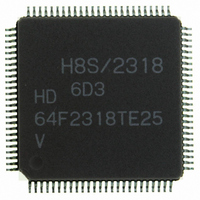
HD64F2318VTE25 Renesas Electronics America, HD64F2318VTE25 Datasheet - Page 776

HD64F2318VTE25
Manufacturer Part Number
HD64F2318VTE25
Description
IC H8S MCU FLASH 256K 100-QFP
Manufacturer
Renesas Electronics America
Series
H8® H8S/2300r
Specifications of HD64F2318VTE25
Core Processor
H8S/2000
Core Size
16-Bit
Speed
25MHz
Connectivity
SCI, SmartCard
Peripherals
POR, PWM, WDT
Number Of I /o
71
Program Memory Size
256KB (256K x 8)
Program Memory Type
FLASH
Ram Size
8K x 8
Voltage - Supply (vcc/vdd)
2.7 V ~ 3.6 V
Data Converters
A/D 8x10b; D/A 2x8b
Oscillator Type
Internal
Operating Temperature
-20°C ~ 75°C
Package / Case
100-TQFP, 100-VQFP
Lead Free Status / RoHS Status
Contains lead / RoHS non-compliant
Eeprom Size
-
- Current page: 776 of 1146
- Download datasheet (7Mb)
Section 17 ROM
Figure 17.77 shows an example of an overlap on block area EB0 of the flash memory.
Emulation is possible for a single area selected from among the eight areas, from EB0 to EB7, of
user MAT bank 0. The area is selected by the setting of the RAM2 to RAM0 bits in the RAMER
register.
(1) To overlap a part of the RAM on area EB0, to allow realtime programming of the data for this
(2) Realtime programming is carried out using the overlaid area of RAM.
In programming or erasing the user MAT, it is necessary to run a program that implements a series
of procedural steps, including the downloading of a on-chip program. In this process, set the
download area with FTDAR so that the overlaid RAM area and the area where the on-chip
program is to be downloaded do not overlap. An FTDAR setting of H'02 will cause part of the
tuned data area to overlap with part of the download area. When using the initial setting of
FTDAR, the data that is to be programmed must be saved beforehand in an area that is not used by
the system.
Rev.7.00 Feb. 14, 2007 page 742 of 1108
REJ09B0089-0700
area, set the RAMER register's RAMS bit to 1, and each of the RAM2 to RAM0 bits to 0.
H'7FFFF
H'00000
H'01000
H'02000
H'03000
H'04000
H'05000
H'06000
H'07000
H'08000
Flash memory
EB8 to EB15
Figure 17.77 Example of a RAM-Overlap Operation
(user MAT)
EB0
EB1
EB2
EB3
EB4
EB5
EB6
EB7
This area is accessible as both a RAM
area and as a flash memory area.
On-chip RAM
H'FFBC00
H'FFDC00
H'FFEBFF
H'FFFBFF
Related parts for HD64F2318VTE25
Image
Part Number
Description
Manufacturer
Datasheet
Request
R

Part Number:
Description:
KIT STARTER FOR M16C/29
Manufacturer:
Renesas Electronics America
Datasheet:

Part Number:
Description:
KIT STARTER FOR R8C/2D
Manufacturer:
Renesas Electronics America
Datasheet:

Part Number:
Description:
R0K33062P STARTER KIT
Manufacturer:
Renesas Electronics America
Datasheet:

Part Number:
Description:
KIT STARTER FOR R8C/23 E8A
Manufacturer:
Renesas Electronics America
Datasheet:

Part Number:
Description:
KIT STARTER FOR R8C/25
Manufacturer:
Renesas Electronics America
Datasheet:

Part Number:
Description:
KIT STARTER H8S2456 SHARPE DSPLY
Manufacturer:
Renesas Electronics America
Datasheet:

Part Number:
Description:
KIT STARTER FOR R8C38C
Manufacturer:
Renesas Electronics America
Datasheet:

Part Number:
Description:
KIT STARTER FOR R8C35C
Manufacturer:
Renesas Electronics America
Datasheet:

Part Number:
Description:
KIT STARTER FOR R8CL3AC+LCD APPS
Manufacturer:
Renesas Electronics America
Datasheet:

Part Number:
Description:
KIT STARTER FOR RX610
Manufacturer:
Renesas Electronics America
Datasheet:

Part Number:
Description:
KIT STARTER FOR R32C/118
Manufacturer:
Renesas Electronics America
Datasheet:

Part Number:
Description:
KIT DEV RSK-R8C/26-29
Manufacturer:
Renesas Electronics America
Datasheet:

Part Number:
Description:
KIT STARTER FOR SH7124
Manufacturer:
Renesas Electronics America
Datasheet:

Part Number:
Description:
KIT STARTER FOR H8SX/1622
Manufacturer:
Renesas Electronics America
Datasheet:

Part Number:
Description:
KIT DEV FOR SH7203
Manufacturer:
Renesas Electronics America
Datasheet:


