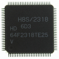
HD64F2318VTE25 Renesas Electronics America, HD64F2318VTE25 Datasheet - Page 548

HD64F2318VTE25
Manufacturer Part Number
HD64F2318VTE25
Description
IC H8S MCU FLASH 256K 100-QFP
Manufacturer
Renesas Electronics America
Series
H8® H8S/2300r
Specifications of HD64F2318VTE25
Core Processor
H8S/2000
Core Size
16-Bit
Speed
25MHz
Connectivity
SCI, SmartCard
Peripherals
POR, PWM, WDT
Number Of I /o
71
Program Memory Size
256KB (256K x 8)
Program Memory Type
FLASH
Ram Size
8K x 8
Voltage - Supply (vcc/vdd)
2.7 V ~ 3.6 V
Data Converters
A/D 8x10b; D/A 2x8b
Oscillator Type
Internal
Operating Temperature
-20°C ~ 75°C
Package / Case
100-TQFP, 100-VQFP
Lead Free Status / RoHS Status
Contains lead / RoHS non-compliant
Eeprom Size
-
- Current page: 548 of 1146
- Download datasheet (7Mb)
Section 13 Smart Card Interface
Bits CKE1 and CKE0 specify the clock output. When the GM bit in SMR is cleared to 0, set these
bits to B'00 if a clock is not to be output, or to B'01 if a clock is to be output. When the GM bit in
SMR is set to 1, clock output is performed. The clock output can also be fixed high or low.
Smart Card Mode Register (SCMR) Settings: The SDIR bit is cleared to 0 if the IC card is of
the direct convention type, and set to 1 if of the inverse convention type.
The SINV bit is cleared to 0 if the IC card is of the direct convention type, and set to 1 if of the
inverse convention type.
The SMIF bit is set to 1 when the smart card interface is used.
Examples of register settings and the waveform of the start character are shown below for the two
types of IC card (direct convention and inverse convention).
• Direct convention (SDIR = SINV = O/E = 0)
• Inverse convention (SDIR = SINV = O/E = 1)
Rev.7.00 Feb. 14, 2007 page 514 of 1108
REJ09B0089-0700
With the direct convention type, the logic 1 level corresponds to state Z and the logic 0 level to
state A, and transfer is performed in LSB-first order. The start character data above is H'3B.
The parity bit is 1 since even parity is stipulated for the smart card.
With the inverse convention type, the logic 1 level corresponds to state A and the logic 0 level
to state Z, and transfer is performed in MSB-first order. The start character data above is H'3F.
The parity bit is 0, corresponding to state Z, since even parity is stipulated for the smart card.
With the chip, inversion specified by the SINV bit applies only to the data bits, D7 to D0. For
parity bit inversion, the O/E bit in SMR should be set to odd parity mode (the same applies to
both transmission and reception).
(Z)
(Z)
Ds
Ds
A
A
D0
D7
Z
Z
D1
D6
Z
Z
D2
D5
A
A
D3
D4
A
Z
D4
D3
Z
A
D5
D2
Z
A
D6
D1
A
A
D7
D0
A
A
Dp
Dp
Z
Z
(Z)
(Z)
State
State
Related parts for HD64F2318VTE25
Image
Part Number
Description
Manufacturer
Datasheet
Request
R

Part Number:
Description:
KIT STARTER FOR M16C/29
Manufacturer:
Renesas Electronics America
Datasheet:

Part Number:
Description:
KIT STARTER FOR R8C/2D
Manufacturer:
Renesas Electronics America
Datasheet:

Part Number:
Description:
R0K33062P STARTER KIT
Manufacturer:
Renesas Electronics America
Datasheet:

Part Number:
Description:
KIT STARTER FOR R8C/23 E8A
Manufacturer:
Renesas Electronics America
Datasheet:

Part Number:
Description:
KIT STARTER FOR R8C/25
Manufacturer:
Renesas Electronics America
Datasheet:

Part Number:
Description:
KIT STARTER H8S2456 SHARPE DSPLY
Manufacturer:
Renesas Electronics America
Datasheet:

Part Number:
Description:
KIT STARTER FOR R8C38C
Manufacturer:
Renesas Electronics America
Datasheet:

Part Number:
Description:
KIT STARTER FOR R8C35C
Manufacturer:
Renesas Electronics America
Datasheet:

Part Number:
Description:
KIT STARTER FOR R8CL3AC+LCD APPS
Manufacturer:
Renesas Electronics America
Datasheet:

Part Number:
Description:
KIT STARTER FOR RX610
Manufacturer:
Renesas Electronics America
Datasheet:

Part Number:
Description:
KIT STARTER FOR R32C/118
Manufacturer:
Renesas Electronics America
Datasheet:

Part Number:
Description:
KIT DEV RSK-R8C/26-29
Manufacturer:
Renesas Electronics America
Datasheet:

Part Number:
Description:
KIT STARTER FOR SH7124
Manufacturer:
Renesas Electronics America
Datasheet:

Part Number:
Description:
KIT STARTER FOR H8SX/1622
Manufacturer:
Renesas Electronics America
Datasheet:

Part Number:
Description:
KIT DEV FOR SH7203
Manufacturer:
Renesas Electronics America
Datasheet:


