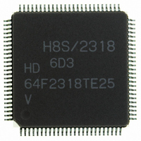
HD64F2318VTE25 Renesas Electronics America, HD64F2318VTE25 Datasheet - Page 990

HD64F2318VTE25
Manufacturer Part Number
HD64F2318VTE25
Description
IC H8S MCU FLASH 256K 100-QFP
Manufacturer
Renesas Electronics America
Series
H8® H8S/2300r
Specifications of HD64F2318VTE25
Core Processor
H8S/2000
Core Size
16-Bit
Speed
25MHz
Connectivity
SCI, SmartCard
Peripherals
POR, PWM, WDT
Number Of I /o
71
Program Memory Size
256KB (256K x 8)
Program Memory Type
FLASH
Ram Size
8K x 8
Voltage - Supply (vcc/vdd)
2.7 V ~ 3.6 V
Data Converters
A/D 8x10b; D/A 2x8b
Oscillator Type
Internal
Operating Temperature
-20°C ~ 75°C
Package / Case
100-TQFP, 100-VQFP
Lead Free Status / RoHS Status
Contains lead / RoHS non-compliant
Eeprom Size
-
- Current page: 990 of 1146
- Download datasheet (7Mb)
Appendix B Internal I/O Registers
Module
Port E
Port F
Port G
Notes: 1.
Rev.7.00 Feb. 14, 2007 page 956 of 1108
REJ09B0089-0700
2.
3.
4.
5.
6.
7.
8.
9.
10. Flash memory registers selection is performed by means of the FLSHE bit in system
11. In modes in which the on-chip flash memory is disabled, a read will return H'00, and
12. In the H8S/2318 F-ZTAT, H8S/2317 F-ZTAT, H8S/2315 F-ZTAT, and H8S/2314 F-
13. In the H8S/2318 F-ZTAT, H8S/2317 F-ZTAT, H8S/2315 F-ZTAT, and H8S/2314 F-
Register
Port E data direction register
Port E data register
Port E register
Port E MOS pull-up control register PEPCR
Port F data direction register
Port F data register
Port F register
Port function control register 1
Port function control register 2
System control register
Port G data register
Port G register
Port function control register 1
Port function control register 2
Lower 16 bits of the address.
Only 0 can be written for flag clearing.
Registers in the DTC cannot be read or written to directly.
Located as register information in on-chip RAM addresses H'EBC0 to H'EFBF. Cannot
be located in external memory space. Do not clear the RAME bit in SYSCR to 0 when
using the DTC.
Determined by the MCU operating mode.
Bits used for pulse output cannot be written to.
Only 0 can be written to bits 7 to 5, to clear the flags.
For information on writing, see section 11.2.4, Notes on Register Access.
Only 0 can be written to bit 7, to clear the flag.
control register 2 (SYSCR2).
writes are invalid. Writes are also disabled when the FWE bit in FLMCR1 is cleared to
0 (except for the H8S/2319 F-ZTAT).
ZTAT when a high level is input to the FWE pin, the initial value is H'80. In the
H8S/2319 F-ZTAT, the initial value is H'80.
ZTAT when a low level is input to the FWE pin, or if a high level is input but the SWE
bit in FLMCR1 is not set, these registers are initialized to H'00.
Port G data direction register
Abbreviation R/W
PEDDR
PEDR
PORTE
PFDDR
PFDR
PORTF
PFCR1
PFCR2
SYSCR
PGDDR
PGDR
PORTG
PFCR1
PFCR2
W
R/W
R
R/W
W
R/W
R
R/W
R/W
R/W
W
R/W
R
R/W
R/W
Initial Value Address *
H'00
H'00
Undefined
H'00
H'80/H'00 *
H'00
Undefined
H'0F
H'30
H'01
H'10/H'00
*
H'00 *
Undefined *
H'0F
H'30
17
*
18
18
17
18
H'FEBD
H'FF6D
H'FF5D
H'FF74
H'FEBE
H'FF6E
H'FF5E
H'FF45
H'FFAC
H'FF39
H'FEBF
H'FF6F
H'FF5F
H'FF45
H'FFAC
1
Related parts for HD64F2318VTE25
Image
Part Number
Description
Manufacturer
Datasheet
Request
R

Part Number:
Description:
KIT STARTER FOR M16C/29
Manufacturer:
Renesas Electronics America
Datasheet:

Part Number:
Description:
KIT STARTER FOR R8C/2D
Manufacturer:
Renesas Electronics America
Datasheet:

Part Number:
Description:
R0K33062P STARTER KIT
Manufacturer:
Renesas Electronics America
Datasheet:

Part Number:
Description:
KIT STARTER FOR R8C/23 E8A
Manufacturer:
Renesas Electronics America
Datasheet:

Part Number:
Description:
KIT STARTER FOR R8C/25
Manufacturer:
Renesas Electronics America
Datasheet:

Part Number:
Description:
KIT STARTER H8S2456 SHARPE DSPLY
Manufacturer:
Renesas Electronics America
Datasheet:

Part Number:
Description:
KIT STARTER FOR R8C38C
Manufacturer:
Renesas Electronics America
Datasheet:

Part Number:
Description:
KIT STARTER FOR R8C35C
Manufacturer:
Renesas Electronics America
Datasheet:

Part Number:
Description:
KIT STARTER FOR R8CL3AC+LCD APPS
Manufacturer:
Renesas Electronics America
Datasheet:

Part Number:
Description:
KIT STARTER FOR RX610
Manufacturer:
Renesas Electronics America
Datasheet:

Part Number:
Description:
KIT STARTER FOR R32C/118
Manufacturer:
Renesas Electronics America
Datasheet:

Part Number:
Description:
KIT DEV RSK-R8C/26-29
Manufacturer:
Renesas Electronics America
Datasheet:

Part Number:
Description:
KIT STARTER FOR SH7124
Manufacturer:
Renesas Electronics America
Datasheet:

Part Number:
Description:
KIT STARTER FOR H8SX/1622
Manufacturer:
Renesas Electronics America
Datasheet:

Part Number:
Description:
KIT DEV FOR SH7203
Manufacturer:
Renesas Electronics America
Datasheet:


