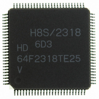
HD64F2318VTE25 Renesas Electronics America, HD64F2318VTE25 Datasheet - Page 658

HD64F2318VTE25
Manufacturer Part Number
HD64F2318VTE25
Description
IC H8S MCU FLASH 256K 100-QFP
Manufacturer
Renesas Electronics America
Series
H8® H8S/2300r
Specifications of HD64F2318VTE25
Core Processor
H8S/2000
Core Size
16-Bit
Speed
25MHz
Connectivity
SCI, SmartCard
Peripherals
POR, PWM, WDT
Number Of I /o
71
Program Memory Size
256KB (256K x 8)
Program Memory Type
FLASH
Ram Size
8K x 8
Voltage - Supply (vcc/vdd)
2.7 V ~ 3.6 V
Data Converters
A/D 8x10b; D/A 2x8b
Oscillator Type
Internal
Operating Temperature
-20°C ~ 75°C
Package / Case
100-TQFP, 100-VQFP
Lead Free Status / RoHS Status
Contains lead / RoHS non-compliant
Eeprom Size
-
- Current page: 658 of 1146
- Download datasheet (7Mb)
Section 17 ROM
FWE application/disconnection (see figures 17.30 to 17.32): FWE application should be carried
out when MCU operation is in a stable condition. If MCU operation is not stable, fix the FWE pin
low and set the protection state.
The following points must be observed concerning FWE application and disconnection to prevent
unintentional programming or erasing of flash memory:
• Apply FWE when the V
• In boot mode, apply and disconnect FWE during a reset.
• In user program mode, FWE can be switched between high and low level regardless of the
• Do not apply FWE if program runaway has occurred.
• Disconnect FWE only when the SWE, ESU, PSU, EV, PV, P, and E bits in FLMCR1 are
Do not apply a constant high level to the FWE pin: Apply a high level to the FWE pin only
when programming or erasing flash memory. A system configuration in which a high level is
constantly applied to the FWE pin should be avoided. Also, while a high level is applied to the
FWE pin, the watchdog timer should be activated to prevent overprogramming or overerasing due
to program runaway, etc.
Use the recommended algorithm when programming and erasing flash memory: The
recommended algorithm enables programming and erasing to be carried out without subjecting the
device to voltage stress or sacrificing program data reliability. When setting the P or E bit in
FLMCR1, the watchdog timer should be set beforehand as a precaution against program runaway,
etc.
Do not set or clear the SWE bit during execution of a program in flash memory: Wait for at
least 100 μs after clearing the SWE bit before executing a program or reading data in flash
memory. When the SWE bit is set, data in flash memory can be rewritten, but when SWE = 1,
flash memory can only be read in program-verify or erase-verify mode. Access flash memory only
for verify operations (verification during programming/erasing). Also, do not clear the SWE bit
during programming, erasing, or verifying.
Similarly, when using the RAM emulation function while a high level is being input to the FWE
pin, the SWE bit must be cleared before executing a program or reading data in flash memory.
Rev.7.00 Feb. 14, 2007 page 624 of 1108
REJ09B0089-0700
Apply FWE when oscillation has stabilized (after the elapse of the oscillation stabilization
time).
reset state. FWE input can also be switched during execution of a program in flash memory.
cleared.
Make sure that the SWE, ESU, PSU, EV, PV, P, and E bits are not set by mistake when
applying or disconnecting FWE.
CC
voltage has stabilized within its rated voltage range.
Related parts for HD64F2318VTE25
Image
Part Number
Description
Manufacturer
Datasheet
Request
R

Part Number:
Description:
KIT STARTER FOR M16C/29
Manufacturer:
Renesas Electronics America
Datasheet:

Part Number:
Description:
KIT STARTER FOR R8C/2D
Manufacturer:
Renesas Electronics America
Datasheet:

Part Number:
Description:
R0K33062P STARTER KIT
Manufacturer:
Renesas Electronics America
Datasheet:

Part Number:
Description:
KIT STARTER FOR R8C/23 E8A
Manufacturer:
Renesas Electronics America
Datasheet:

Part Number:
Description:
KIT STARTER FOR R8C/25
Manufacturer:
Renesas Electronics America
Datasheet:

Part Number:
Description:
KIT STARTER H8S2456 SHARPE DSPLY
Manufacturer:
Renesas Electronics America
Datasheet:

Part Number:
Description:
KIT STARTER FOR R8C38C
Manufacturer:
Renesas Electronics America
Datasheet:

Part Number:
Description:
KIT STARTER FOR R8C35C
Manufacturer:
Renesas Electronics America
Datasheet:

Part Number:
Description:
KIT STARTER FOR R8CL3AC+LCD APPS
Manufacturer:
Renesas Electronics America
Datasheet:

Part Number:
Description:
KIT STARTER FOR RX610
Manufacturer:
Renesas Electronics America
Datasheet:

Part Number:
Description:
KIT STARTER FOR R32C/118
Manufacturer:
Renesas Electronics America
Datasheet:

Part Number:
Description:
KIT DEV RSK-R8C/26-29
Manufacturer:
Renesas Electronics America
Datasheet:

Part Number:
Description:
KIT STARTER FOR SH7124
Manufacturer:
Renesas Electronics America
Datasheet:

Part Number:
Description:
KIT STARTER FOR H8SX/1622
Manufacturer:
Renesas Electronics America
Datasheet:

Part Number:
Description:
KIT DEV FOR SH7203
Manufacturer:
Renesas Electronics America
Datasheet:


