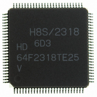
HD64F2318VTE25 Renesas Electronics America, HD64F2318VTE25 Datasheet - Page 575

HD64F2318VTE25
Manufacturer Part Number
HD64F2318VTE25
Description
IC H8S MCU FLASH 256K 100-QFP
Manufacturer
Renesas Electronics America
Series
H8® H8S/2300r
Specifications of HD64F2318VTE25
Core Processor
H8S/2000
Core Size
16-Bit
Speed
25MHz
Connectivity
SCI, SmartCard
Peripherals
POR, PWM, WDT
Number Of I /o
71
Program Memory Size
256KB (256K x 8)
Program Memory Type
FLASH
Ram Size
8K x 8
Voltage - Supply (vcc/vdd)
2.7 V ~ 3.6 V
Data Converters
A/D 8x10b; D/A 2x8b
Oscillator Type
Internal
Operating Temperature
-20°C ~ 75°C
Package / Case
100-TQFP, 100-VQFP
Lead Free Status / RoHS Status
Contains lead / RoHS non-compliant
Eeprom Size
-
- Current page: 575 of 1146
- Download datasheet (7Mb)
14.4
The A/D converter operates by successive approximations with 10-bit resolution. It has two
operating modes: single mode and scan mode.
14.4.1
Single mode is selected when A/D conversion is to be performed on a single channel only. A/D
conversion is started when the ADST bit is set to 1 by software or by external trigger input. The
ADST bit remains set to 1 during A/D conversion, and is automatically cleared to 0 when
conversion ends.
On completion of conversion, the ADF flag is set to 1. If the ADIE bit is set to 1 at this time, an
ADI interrupt request is generated. The ADF flag is cleared by writing 0 to it after reading
ADCSR.
When the operating mode or analog input channel must be changed during analog conversion, to
prevent incorrect operation, first clear the ADST bit to 0 in ADCSR to halt A/D conversion. After
making the necessary changes, set the ADST bit to 1 to start A/D conversion again. The ADST
bit can be set at the same time as the operating mode or input channel is changed.
Typical operations when channel 1 (AN1) is selected in single mode are described next. Figure
14.3 shows a timing diagram for this example.
[1] Single mode is selected (SCAN = 0), input channel AN1 is selected (CH2 = 0, CH1 = 0,
[2] When A/D conversion is completed, the result is transferred to ADDRB. At the same time the
[3] Since ADF = 1 and ADIE = 1, an ADI interrupt is requested.
[4] The A/D interrupt handling routine starts.
[5] The routine reads ADCSR, then writes 0 to the ADF flag.
[6] The routine reads and processes the conversion result (ADDRB).
[7] Execution of the A/D interrupt handling routine ends. After that, if the ADST bit is set to 1,
CH0 = 1), the A/D interrupt is enabled (ADIE = 1), and A/D conversion is started (ADST = 1).
ADF flag is set to 1, the ADST bit is cleared to 0, and the A/D converter becomes idle.
A/D conversion starts again and steps [2] to [7] are repeated.
Operation
Single Mode (SCAN = 0)
Section 14 A/D Converter (8 Analog Input Channel Version)
Rev.7.00 Feb. 14, 2007 page 541 of 1108
REJ09B0089-0700
Related parts for HD64F2318VTE25
Image
Part Number
Description
Manufacturer
Datasheet
Request
R

Part Number:
Description:
KIT STARTER FOR M16C/29
Manufacturer:
Renesas Electronics America
Datasheet:

Part Number:
Description:
KIT STARTER FOR R8C/2D
Manufacturer:
Renesas Electronics America
Datasheet:

Part Number:
Description:
R0K33062P STARTER KIT
Manufacturer:
Renesas Electronics America
Datasheet:

Part Number:
Description:
KIT STARTER FOR R8C/23 E8A
Manufacturer:
Renesas Electronics America
Datasheet:

Part Number:
Description:
KIT STARTER FOR R8C/25
Manufacturer:
Renesas Electronics America
Datasheet:

Part Number:
Description:
KIT STARTER H8S2456 SHARPE DSPLY
Manufacturer:
Renesas Electronics America
Datasheet:

Part Number:
Description:
KIT STARTER FOR R8C38C
Manufacturer:
Renesas Electronics America
Datasheet:

Part Number:
Description:
KIT STARTER FOR R8C35C
Manufacturer:
Renesas Electronics America
Datasheet:

Part Number:
Description:
KIT STARTER FOR R8CL3AC+LCD APPS
Manufacturer:
Renesas Electronics America
Datasheet:

Part Number:
Description:
KIT STARTER FOR RX610
Manufacturer:
Renesas Electronics America
Datasheet:

Part Number:
Description:
KIT STARTER FOR R32C/118
Manufacturer:
Renesas Electronics America
Datasheet:

Part Number:
Description:
KIT DEV RSK-R8C/26-29
Manufacturer:
Renesas Electronics America
Datasheet:

Part Number:
Description:
KIT STARTER FOR SH7124
Manufacturer:
Renesas Electronics America
Datasheet:

Part Number:
Description:
KIT STARTER FOR H8SX/1622
Manufacturer:
Renesas Electronics America
Datasheet:

Part Number:
Description:
KIT DEV FOR SH7203
Manufacturer:
Renesas Electronics America
Datasheet:


