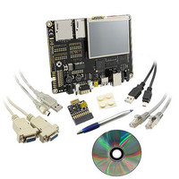
BMSKTOPASA900(DCE) Toshiba, BMSKTOPASA900(DCE) Datasheet - Page 132

BMSKTOPASA900(DCE)
Manufacturer Part Number
BMSKTOPASA900(DCE)
Description
KIT STARTER TMPA900 USB JTAG
Manufacturer
Toshiba
Series
TOPASr
Type
MCUr
Specifications of BMSKTOPASA900(DCE)
Contents
Evaluation Board, Cable(s), Software and Documentation
For Use With/related Products
TMPA900CMXBG
Lead Free Status / RoHS Status
Lead free / RoHS Compliant
- Current page: 132 of 959
- Download datasheet (5Mb)
GPIOADATA
Reserved
Reserved
Reserved
GPIOAIS
GPIOAIBE
GPIOAIEV
GPIOAIE
GPIOARIS
GPIOAMIS
GPIOAIC
General-purpose input
Key input
3.9.2
Register
Bit 7
Bit7
Name
Function
Function
3.9.2.1
Note: All bits are provided with pull up resisters.
Note: All bits support the interrupt function. All bits are provided with pull up resisters.
General-purpose input setting
Key input function setting
input pin.
general-purpose ports. Each port should basically be accessed in word (32-bit) units.
Port Function Settings
Port A can be used not only as a general-purpose input pin with pull up but also as key
By enabling interrupts, Port A is used as key input pins (KI3-KI0).
Port A can be used without pull up. Please refer to Section 3.26 PMC.
This section describes the settings of Port A through Port V that can also function as
Bit 6
Bit6
Port A
0x03FC
0x0400
0x0424
0x0428
0x0804
0x0808
0x080C
0x0810
0x0814
0x0818
0x081C
Address
(base+)
Interrupt Enable
Interrupt Enable
GPIOAIE
GPIOAIE
Bit 5
0
1
Bit5
PortA Data Regisiter
Port A Interrupt Select Register (Level and Edge)
Port A Interrupt Select Register (Single edge and Both edge)
Port A Interrupt Select Register
(Falling edge/Low level and Rising edge/High level)
Port A Interrupt Enable Register
Port A Interrupt Status Register (Raw)
Port A Interrupt Status Register (Masked)
Port A Interrupt Clear Register
TENTATIVE
Bit 4
TMPA900CM-131
Bit4
Input
Bit 3
Bit3
KI3
Description
Input
Bit 2
Bit2
KI2
Base address = 0xF080_0000
Input
Bit 1
Bit1
KI1
TMPA900CM
2009-10-14
Input
Bit 0
Bit0
KI0
Related parts for BMSKTOPASA900(DCE)
Image
Part Number
Description
Manufacturer
Datasheet
Request
R
Part Number:
Description:
Toshiba Semiconductor [TOSHIBA IGBT Module Silicon N Channel IGBT]
Manufacturer:
TOSHIBA Semiconductor CORPORATION
Datasheet:
Part Number:
Description:
TOSHIBA GTR MODULE SILICON NPN TRIPLE DIFFUSED TYPE
Manufacturer:
TOSHIBA Semiconductor CORPORATION
Datasheet:
Part Number:
Description:
TOSHIBA GTR Module Silicon N Channel IGBT
Manufacturer:
TOSHIBA Semiconductor CORPORATION
Datasheet:
Part Number:
Description:
TOSHIBA Intelligent Power Module Silicon N Channel IGBT
Manufacturer:
TOSHIBA Semiconductor CORPORATION
Datasheet:
Part Number:
Description:
TOSHIBA INTELLIGENT POWER MODULE SILICON N CHANNEL LGBT
Manufacturer:
TOSHIBA Semiconductor CORPORATION
Datasheet:
Part Number:
Description:
TOSHIBA IGBT Module Silicon N Channel IGBT
Manufacturer:
TOSHIBA Semiconductor CORPORATION
Datasheet:
Part Number:
Description:
TOSHIBA GTR MODULE SILICON N−CHANNEL IGBT
Manufacturer:
TOSHIBA Semiconductor CORPORATION
Datasheet:
Part Number:
Description:
TOSHIBA Intelligent Power Module Silicon N Channel IGBT
Manufacturer:
TOSHIBA Semiconductor CORPORATION
Datasheet:
Part Number:
Description:
TOSHIBA GTR Module Silicon N Channel IGBT
Manufacturer:
TOSHIBA Semiconductor CORPORATION
Datasheet:
Part Number:
Description:
TOSHIBA INTELLIGENT POWER MODULE
Manufacturer:
TOSHIBA Semiconductor CORPORATION
Datasheet:
Part Number:
Description:
TOSHIBA Intelligent Power Module Silicon N Channel IGBT
Manufacturer:
TOSHIBA Semiconductor CORPORATION
Datasheet:
Part Number:
Description:
TOSHIBA Intelligent Power Module Silicon N Channel IGBT
Manufacturer:
TOSHIBA Semiconductor CORPORATION
Datasheet:
Part Number:
Description:
TOSHIBA IGBT Module Silicon N Channel IGBT
Manufacturer:
TOSHIBA Semiconductor CORPORATION
Datasheet:
Part Number:
Description:
TOSHIBA Intelligent Power Module Silicon N Channel IGBT
Manufacturer:
TOSHIBA Semiconductor CORPORATION
Datasheet:
Part Number:
Description:
Toshiba Semiconductor [SILICON N CHANNEL 1GBT]
Manufacturer:
TOSHIBA Semiconductor CORPORATION
Datasheet:


