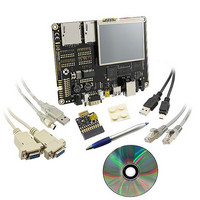
BMSKTOPASA900(DCE) Toshiba, BMSKTOPASA900(DCE) Datasheet - Page 14

BMSKTOPASA900(DCE)
Manufacturer Part Number
BMSKTOPASA900(DCE)
Description
KIT STARTER TMPA900 USB JTAG
Manufacturer
Toshiba
Series
TOPASr
Type
MCUr
Specifications of BMSKTOPASA900(DCE)
Contents
Evaluation Board, Cable(s), Software and Documentation
For Use With/related Products
TMPA900CMXBG
Lead Free Status / RoHS Status
Lead free / RoHS Compliant
- Current page: 14 of 959
- Download datasheet (5Mb)
SA0 to SA7
D0 to D7
SB0 to SB7
D8 to D15
SC0 to SC7
D16 to D23
SD0 to SD7
D24 to D31
SE0 to SE7
A0 to A7
SF0 to SF7
A8 to A15
SG0 to SG7
A16 to A23
−
SH2
SMCBE0n
SK5
SMCBE1n
SK6
SMCBE2n
SK7
SMCBE3n
SH3
SMCCS0n
SH4
SMCCS1n
−
−
SH7
DMCCSn
DMCCSn
SJ0
SMCOEn
SJ1
DMCWEn
DMCWEn
SJ2
DMCRASn
DMCRASn
2.2
Pin name
Pin Names and Functions
depending on the status of the external pin “SELMEMC”.
The names and functions of I/O pins are shown below.
Pins associated with memory are switched to either of two types of MPMC (MPMC0/1)
Note: Pin names "SA0 through SA7, …, and SU0 through SU4" are symbols used for convenience and are different
Number of pins
from general-purpose port functions "PA0 through PA3, …, and PV0 through PV7."
8
8
8
8
8
8
8
1
1
1
1
1
1
1
1
1
1
−
Input/Output
−
Input/Output
−
Input/Output
−
Input/Output
−
Output
−
Output
−
Output
−
Output
−
Output
−
Output
−
Output
−
Output
−
Output
−
Output
Output
−
Output
−
Output
Output
−
Output
Output
Input/Output
Table 2.2.1 Pin names and functions (1/8)
−
Data: Data bus D0 to D7
−
Data: Data bus D8 to D15
-
Data: Data bus D16 to D23
-
Data: Data bus D24 to D31
−
Address: Address bus A0 to A7
−
Address: Address bus A8 to A15
−
Address: Address bus A16 to A23
−
Byte enable signal (D0 to D7) for
NORF/SRAM/MROM
−
Byte enable signal (D8 to D15) for
NORF/SRAM/MROM
−
Byte enable signal (D16 to D23) for
NORF/SRAM/MROM
−
Byte enable signal (D24 to D31) for
NORF/SRAM/MROM
−
Chip select signal 0 for NORF/SRAM/MROM
−
Chip select signal 1 for NORF/SRAM/MROM
−
Write-enable signal for SDR_SDRAM
Write-enable signal for DDR_SDRAM
−
Out-enable signal for NORF/SRAM/MROM
−
Write-enable signal for SDR_SDRAM
Write-enable signal for DDR_SDRAM
−
Row address strobe signal for SDR_SDRAM
Row address strobe signal for DDR_SDRAM
TENTATIVE
TMPA900CM- 13
Function
−
For both MPMC0 and MPMC1
−
For both MPMC0 and MPMC1
−
For both MPMC0 and MPMC1
−
For both MPMC0 and MPMC1
−
For both MPMC0 and MPMC1
−
For both MPMC0 and MPMC1
−
For both MPMC0 and MPMC1
−
For both MPMC0 and MPMC1
−
For both MPMC0 and MPMC1
−
For both MPMC0 and MPMC1
−
For both MPMC0 and MPMC1
−
For both MPMC0 and MPMC1
−
For both MPMC0 and MPMC1
−
When using MPMC0
When using MPMC1
−
For both MPMC0 and MPMC1
−
When using MPMC0
When using MPMC1
−
When using MPMC0
When using MPMC1
Remarks
TMPA900CM
2009-10-14
Related parts for BMSKTOPASA900(DCE)
Image
Part Number
Description
Manufacturer
Datasheet
Request
R
Part Number:
Description:
Toshiba Semiconductor [TOSHIBA IGBT Module Silicon N Channel IGBT]
Manufacturer:
TOSHIBA Semiconductor CORPORATION
Datasheet:
Part Number:
Description:
TOSHIBA GTR MODULE SILICON NPN TRIPLE DIFFUSED TYPE
Manufacturer:
TOSHIBA Semiconductor CORPORATION
Datasheet:
Part Number:
Description:
TOSHIBA GTR Module Silicon N Channel IGBT
Manufacturer:
TOSHIBA Semiconductor CORPORATION
Datasheet:
Part Number:
Description:
TOSHIBA Intelligent Power Module Silicon N Channel IGBT
Manufacturer:
TOSHIBA Semiconductor CORPORATION
Datasheet:
Part Number:
Description:
TOSHIBA INTELLIGENT POWER MODULE SILICON N CHANNEL LGBT
Manufacturer:
TOSHIBA Semiconductor CORPORATION
Datasheet:
Part Number:
Description:
TOSHIBA IGBT Module Silicon N Channel IGBT
Manufacturer:
TOSHIBA Semiconductor CORPORATION
Datasheet:
Part Number:
Description:
TOSHIBA GTR MODULE SILICON N−CHANNEL IGBT
Manufacturer:
TOSHIBA Semiconductor CORPORATION
Datasheet:
Part Number:
Description:
TOSHIBA Intelligent Power Module Silicon N Channel IGBT
Manufacturer:
TOSHIBA Semiconductor CORPORATION
Datasheet:
Part Number:
Description:
TOSHIBA GTR Module Silicon N Channel IGBT
Manufacturer:
TOSHIBA Semiconductor CORPORATION
Datasheet:
Part Number:
Description:
TOSHIBA INTELLIGENT POWER MODULE
Manufacturer:
TOSHIBA Semiconductor CORPORATION
Datasheet:
Part Number:
Description:
TOSHIBA Intelligent Power Module Silicon N Channel IGBT
Manufacturer:
TOSHIBA Semiconductor CORPORATION
Datasheet:
Part Number:
Description:
TOSHIBA Intelligent Power Module Silicon N Channel IGBT
Manufacturer:
TOSHIBA Semiconductor CORPORATION
Datasheet:
Part Number:
Description:
TOSHIBA IGBT Module Silicon N Channel IGBT
Manufacturer:
TOSHIBA Semiconductor CORPORATION
Datasheet:
Part Number:
Description:
TOSHIBA Intelligent Power Module Silicon N Channel IGBT
Manufacturer:
TOSHIBA Semiconductor CORPORATION
Datasheet:
Part Number:
Description:
Toshiba Semiconductor [SILICON N CHANNEL 1GBT]
Manufacturer:
TOSHIBA Semiconductor CORPORATION
Datasheet:


