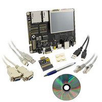
BMSKTOPASA900(DCE) Toshiba, BMSKTOPASA900(DCE) Datasheet - Page 458

BMSKTOPASA900(DCE)
Manufacturer Part Number
BMSKTOPASA900(DCE)
Description
KIT STARTER TMPA900 USB JTAG
Manufacturer
Toshiba
Series
TOPASr
Type
MCUr
Specifications of BMSKTOPASA900(DCE)
Contents
Evaluation Board, Cable(s), Software and Documentation
For Use With/related Products
TMPA900CMXBG
Lead Free Status / RoHS Status
Lead free / RoHS Compliant
- Current page: 458 of 959
- Download datasheet (5Mb)
3.15.2
two channels operate identically, operational descriptions are provided for channel 0 only.
types of synchronous serial interfaces.
transmit and receive paths are buffered with a 16-bit wide, 8 locations deep independent
transmit FIFO and receive FIFO in transmit mode and receive mode, respectively. Serial data
is transmitted on SP0DO and received on SP0DI.
the input clock PCLK. The SSP operating mode, frame format and size are programmed
through the control registers SSP0CR0 and SSP0CR1.
This LSI contains the SSP comprised of two channels (channel 0 and channel 1). Since the
The SSP is an interface for serial communication with peripheral devices that have three
The SSP performs serial-to-parallel conversion on data received from a peripheral device. The
The SSP contains a programmable prescaler to generate the serial output clock SP0CLK from
free-running counters is used to provide the serial output clock SP0CLK.
PCLK by a factor of 2 to 254 in steps of two. By not using the least significant bit of the
SSP0CPSR register, division by an odd number cannot be programmed.
one to the value programmed in the SSP0CR0 control register, to give the master output
clock SP0CLK.
SSP Overview
(1) Clock prescaler
When configured as a master, a clock prescaler comprising two serially linked
This clock prescaler can be programmed, through the SSP0CPSR register, to divide
The output of the prescaler is further divided by a factor of 1 to 256, obtained by adding
Bit rate = f
PCLK
(Depends on the setting.)
PCLK
CPSDVSR [7:1]
Clock initial value
Clock prescaler
Figure 3.15.2 Block diagram of Clock prescaler
/ (CPSDVSR × (1 + SCR))
TENTATIVE
TMPA900CM- 457
SSPCLKDIV
(SCR [7:0] + 1)
Toggle circuit
Divide circuit
Clock inversion trigger
SPxCLK
TMPA900CM
2009-10-14
Related parts for BMSKTOPASA900(DCE)
Image
Part Number
Description
Manufacturer
Datasheet
Request
R
Part Number:
Description:
Toshiba Semiconductor [TOSHIBA IGBT Module Silicon N Channel IGBT]
Manufacturer:
TOSHIBA Semiconductor CORPORATION
Datasheet:
Part Number:
Description:
TOSHIBA GTR MODULE SILICON NPN TRIPLE DIFFUSED TYPE
Manufacturer:
TOSHIBA Semiconductor CORPORATION
Datasheet:
Part Number:
Description:
TOSHIBA GTR Module Silicon N Channel IGBT
Manufacturer:
TOSHIBA Semiconductor CORPORATION
Datasheet:
Part Number:
Description:
TOSHIBA Intelligent Power Module Silicon N Channel IGBT
Manufacturer:
TOSHIBA Semiconductor CORPORATION
Datasheet:
Part Number:
Description:
TOSHIBA INTELLIGENT POWER MODULE SILICON N CHANNEL LGBT
Manufacturer:
TOSHIBA Semiconductor CORPORATION
Datasheet:
Part Number:
Description:
TOSHIBA IGBT Module Silicon N Channel IGBT
Manufacturer:
TOSHIBA Semiconductor CORPORATION
Datasheet:
Part Number:
Description:
TOSHIBA GTR MODULE SILICON N−CHANNEL IGBT
Manufacturer:
TOSHIBA Semiconductor CORPORATION
Datasheet:
Part Number:
Description:
TOSHIBA Intelligent Power Module Silicon N Channel IGBT
Manufacturer:
TOSHIBA Semiconductor CORPORATION
Datasheet:
Part Number:
Description:
TOSHIBA GTR Module Silicon N Channel IGBT
Manufacturer:
TOSHIBA Semiconductor CORPORATION
Datasheet:
Part Number:
Description:
TOSHIBA INTELLIGENT POWER MODULE
Manufacturer:
TOSHIBA Semiconductor CORPORATION
Datasheet:
Part Number:
Description:
TOSHIBA Intelligent Power Module Silicon N Channel IGBT
Manufacturer:
TOSHIBA Semiconductor CORPORATION
Datasheet:
Part Number:
Description:
TOSHIBA Intelligent Power Module Silicon N Channel IGBT
Manufacturer:
TOSHIBA Semiconductor CORPORATION
Datasheet:
Part Number:
Description:
TOSHIBA IGBT Module Silicon N Channel IGBT
Manufacturer:
TOSHIBA Semiconductor CORPORATION
Datasheet:
Part Number:
Description:
TOSHIBA Intelligent Power Module Silicon N Channel IGBT
Manufacturer:
TOSHIBA Semiconductor CORPORATION
Datasheet:
Part Number:
Description:
Toshiba Semiconductor [SILICON N CHANNEL 1GBT]
Manufacturer:
TOSHIBA Semiconductor CORPORATION
Datasheet:


