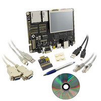
BMSKTOPASA900(DCE) Toshiba, BMSKTOPASA900(DCE) Datasheet - Page 3

BMSKTOPASA900(DCE)
Manufacturer Part Number
BMSKTOPASA900(DCE)
Description
KIT STARTER TMPA900 USB JTAG
Manufacturer
Toshiba
Series
TOPASr
Type
MCUr
Specifications of BMSKTOPASA900(DCE)
Contents
Evaluation Board, Cable(s), Software and Documentation
For Use With/related Products
TMPA900CMXBG
Lead Free Status / RoHS Status
Lead free / RoHS Compliant
- Current page: 3 of 959
- Download datasheet (5Mb)
This device has SFR (Special Function Register) each IP (Peripheral circuits). SFR is shown as following
in this data book.
a) IP lists
SAMPLE
・・・
[31:8]
[7:6]
・・・
b) SFR (register) description
Register
Bit
Name
・ IP lists show the register name, address and easy descriptions.
・ 32bit address is assigned to all registers. It shows as [base address + (specific) address].
・ Basically, each register is structured 32 bit register. (There is a part of exception.)
・ Each description shows Bit, Bit Symbol, Type, Reset value and Description.
Note1: Case of this register (SAMPLE): 00000001 address because 00000000 address (hex)+0001 address (hex)
Note2: This register is sample register. There is not this data book.
Note1: Basically 3types.
Note2: Bit state description:
Note3: 1 Word = 32 bit.
−
SAMPLE76
・・・
Symbol
R/W(READ/WRITE): Enable Read/Write
RO(READ ONLY):
WO(WRITE ONLY):
There are exception types (USB device controller and SD host controller).
Please refer to those sections.
Hexadecimal:
Binary:
Bit
・・・
Address
(base+)
0x0001
−
R/W
・・・
Type
- Introduction - Notes on the registers -
Sample register
・・・
Enable Read only
Enable Write only
0x00FF = 255 (Decimal)
0y0101 = 5 (Decimal)
Undefined
0y00
・・・
Reset
Value
TENTATIVE
TMPA900CM- 2
Read undefined. Write as zero.
Sample setting
0y00: Set to Sample mode 0
0y01: Set to Sample mode 1
0y10: Set to Sample mode 2
0y11: Set to Sample mode 3
・・・
Description
Description
Address = (0x0000_0000) + (0x0001)
base address = 0x0000_0000
TMPA900CM
2009-10-14
Related parts for BMSKTOPASA900(DCE)
Image
Part Number
Description
Manufacturer
Datasheet
Request
R
Part Number:
Description:
Toshiba Semiconductor [TOSHIBA IGBT Module Silicon N Channel IGBT]
Manufacturer:
TOSHIBA Semiconductor CORPORATION
Datasheet:
Part Number:
Description:
TOSHIBA GTR MODULE SILICON NPN TRIPLE DIFFUSED TYPE
Manufacturer:
TOSHIBA Semiconductor CORPORATION
Datasheet:
Part Number:
Description:
TOSHIBA GTR Module Silicon N Channel IGBT
Manufacturer:
TOSHIBA Semiconductor CORPORATION
Datasheet:
Part Number:
Description:
TOSHIBA Intelligent Power Module Silicon N Channel IGBT
Manufacturer:
TOSHIBA Semiconductor CORPORATION
Datasheet:
Part Number:
Description:
TOSHIBA INTELLIGENT POWER MODULE SILICON N CHANNEL LGBT
Manufacturer:
TOSHIBA Semiconductor CORPORATION
Datasheet:
Part Number:
Description:
TOSHIBA IGBT Module Silicon N Channel IGBT
Manufacturer:
TOSHIBA Semiconductor CORPORATION
Datasheet:
Part Number:
Description:
TOSHIBA GTR MODULE SILICON N−CHANNEL IGBT
Manufacturer:
TOSHIBA Semiconductor CORPORATION
Datasheet:
Part Number:
Description:
TOSHIBA Intelligent Power Module Silicon N Channel IGBT
Manufacturer:
TOSHIBA Semiconductor CORPORATION
Datasheet:
Part Number:
Description:
TOSHIBA GTR Module Silicon N Channel IGBT
Manufacturer:
TOSHIBA Semiconductor CORPORATION
Datasheet:
Part Number:
Description:
TOSHIBA INTELLIGENT POWER MODULE
Manufacturer:
TOSHIBA Semiconductor CORPORATION
Datasheet:
Part Number:
Description:
TOSHIBA Intelligent Power Module Silicon N Channel IGBT
Manufacturer:
TOSHIBA Semiconductor CORPORATION
Datasheet:
Part Number:
Description:
TOSHIBA Intelligent Power Module Silicon N Channel IGBT
Manufacturer:
TOSHIBA Semiconductor CORPORATION
Datasheet:
Part Number:
Description:
TOSHIBA IGBT Module Silicon N Channel IGBT
Manufacturer:
TOSHIBA Semiconductor CORPORATION
Datasheet:
Part Number:
Description:
TOSHIBA Intelligent Power Module Silicon N Channel IGBT
Manufacturer:
TOSHIBA Semiconductor CORPORATION
Datasheet:
Part Number:
Description:
Toshiba Semiconductor [SILICON N CHANNEL 1GBT]
Manufacturer:
TOSHIBA Semiconductor CORPORATION
Datasheet:


