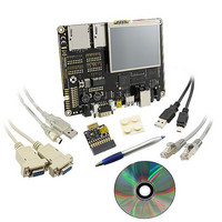
BMSKTOPASA900(DCE) Toshiba, BMSKTOPASA900(DCE) Datasheet - Page 949

BMSKTOPASA900(DCE)
Manufacturer Part Number
BMSKTOPASA900(DCE)
Description
KIT STARTER TMPA900 USB JTAG
Manufacturer
Toshiba
Series
TOPASr
Type
MCUr
Specifications of BMSKTOPASA900(DCE)
Contents
Evaluation Board, Cable(s), Software and Documentation
For Use With/related Products
TMPA900CMXBG
Lead Free Status / RoHS Status
Lead free / RoHS Compliant
- Current page: 949 of 959
- Download datasheet (5Mb)
AC measurement conditions:
SPxCLK Period (Master)
SPxCLK Period (Slave)
SPxCLK rise up time
SPxCLK fall down time
Master mode: SPxCLK low level pulse width
Master mode: SPxCLK high level pulse width
Master Mode:
Master Mode:
Master Mode:
Master Mode:
Master Mode:
Slave mode:
Slave mode:
Slave mode:
Slave mode:
Slave mode:
Slave mode: SPxCLK low level pulse width
Slave mode: SPxCLK high level pulse width
Load capacitance CL = 25 pF
4.3.7
SPxCLK rise/fall to output data valid
SPxCLK rise/fall to output data hold
SPxCLK rise/fall to input data valid delay time
SPxCLK rise/fall to input data hold
SPxFSS valid to SPxCLK rise/fall
SPxCLK rise/fall to output data valid delay time
SPxCLK rise/fall to output data hold
SPxCLK rise/fall to input data valid delay time
SPxCLK rise/fall to input data hold
SPxFSS valid to SPxCLK rise/fall
Note1: Baud rate Clock is set under below condition
Note: The “Equation” column in the table shows the specifications under the conditions DVCC3IO = 3.0 to 3.6 V and
AC measurement conditions
Master mode
Slave Mode
• Output level: High = 0.7 × DVC3IOM, Low = 0.3 × DVCC3IO
• Input level: High = 0.9 × DVCC3IO, Low = 0.1× DVCC3IO
SSP Controller
• The letter “T” used in the equations in the table represents the period of internal bus frequency (f
m = (<CPSDVSR> × (1 + <SCR>)) = f
<CPSDVR> is set only even number and “m” must set during 65204
n = f
which is one-half of the CPU clock (f
DVCC1A = DVCC1B = DVCC1C = 1.4 to 1.6 V.
70 degree.
to 85 degree.
The internal bus cycle is T=10ns minimum value when the guaranteed temperature is 0 to
The internal bus cycle is T=13.3ns minimum value when the guaranteed temperature is -20
Parameter
PCLK
/SPxCLK (65204 ≥ n ≥ 12 )
TMPA900CM- 948
TENTATIVE
Symbol
t
t
t
t
t
t
t
t
t
t
t
ODSM
ODHM
t
t
t
ODSS
ODHS
OFSM
Note1)
WHM
IDSM
IDHM
OFSS
WLM
WHS
IDSS
IDHS
WLS
T
FCLK
T
t
t
r
m
f
s
).
PCLK
However more than
/SPxCLK
(m)T / 2 - 7.0
(m)T / 2 –7.0
(n)T /2 + (2T)
(n)T / 2 - 7.0
(n)T / 2 - 7.0
(m)T/2 -10
(3T) + 10
(m)T -10
(m)T
50ns
Min
(n)T
(n)T
5.0
Equation
≥
(n)T /2 + (3T)
(m)T /2 - 20
m
(m)T + 10
(3T) + 25
- 10.0
≥
Max
10.0
10.0
15.0
2
100MHz
PCLK
(m=6
10.0
50∼70
n=12)
120.0
60.0
10.0
10.0
23.0
23.0
53.0
53.0
15.0
20.0
55.0
80.0
80.0
40.0
120
5.0
TMPA900CM
2009-10-14
52.5∼72.5
96MHz
PCLK
n=12)
(m=6
125.0
62.5
10.0
10.0
24.3
24.3
55.5
55.5
15.0
21.3
11.2
56.3
83.3
83.8
41.3
125
5.0
PCLK
),
Unit
ns
Related parts for BMSKTOPASA900(DCE)
Image
Part Number
Description
Manufacturer
Datasheet
Request
R
Part Number:
Description:
Toshiba Semiconductor [TOSHIBA IGBT Module Silicon N Channel IGBT]
Manufacturer:
TOSHIBA Semiconductor CORPORATION
Datasheet:
Part Number:
Description:
TOSHIBA GTR MODULE SILICON NPN TRIPLE DIFFUSED TYPE
Manufacturer:
TOSHIBA Semiconductor CORPORATION
Datasheet:
Part Number:
Description:
TOSHIBA GTR Module Silicon N Channel IGBT
Manufacturer:
TOSHIBA Semiconductor CORPORATION
Datasheet:
Part Number:
Description:
TOSHIBA Intelligent Power Module Silicon N Channel IGBT
Manufacturer:
TOSHIBA Semiconductor CORPORATION
Datasheet:
Part Number:
Description:
TOSHIBA INTELLIGENT POWER MODULE SILICON N CHANNEL LGBT
Manufacturer:
TOSHIBA Semiconductor CORPORATION
Datasheet:
Part Number:
Description:
TOSHIBA IGBT Module Silicon N Channel IGBT
Manufacturer:
TOSHIBA Semiconductor CORPORATION
Datasheet:
Part Number:
Description:
TOSHIBA GTR MODULE SILICON N−CHANNEL IGBT
Manufacturer:
TOSHIBA Semiconductor CORPORATION
Datasheet:
Part Number:
Description:
TOSHIBA Intelligent Power Module Silicon N Channel IGBT
Manufacturer:
TOSHIBA Semiconductor CORPORATION
Datasheet:
Part Number:
Description:
TOSHIBA GTR Module Silicon N Channel IGBT
Manufacturer:
TOSHIBA Semiconductor CORPORATION
Datasheet:
Part Number:
Description:
TOSHIBA INTELLIGENT POWER MODULE
Manufacturer:
TOSHIBA Semiconductor CORPORATION
Datasheet:
Part Number:
Description:
TOSHIBA Intelligent Power Module Silicon N Channel IGBT
Manufacturer:
TOSHIBA Semiconductor CORPORATION
Datasheet:
Part Number:
Description:
TOSHIBA Intelligent Power Module Silicon N Channel IGBT
Manufacturer:
TOSHIBA Semiconductor CORPORATION
Datasheet:
Part Number:
Description:
TOSHIBA IGBT Module Silicon N Channel IGBT
Manufacturer:
TOSHIBA Semiconductor CORPORATION
Datasheet:
Part Number:
Description:
TOSHIBA Intelligent Power Module Silicon N Channel IGBT
Manufacturer:
TOSHIBA Semiconductor CORPORATION
Datasheet:
Part Number:
Description:
Toshiba Semiconductor [SILICON N CHANNEL 1GBT]
Manufacturer:
TOSHIBA Semiconductor CORPORATION
Datasheet:


