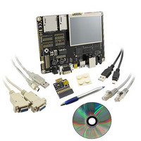
BMSKTOPASA900(DCE) Toshiba, BMSKTOPASA900(DCE) Datasheet - Page 219

BMSKTOPASA900(DCE)
Manufacturer Part Number
BMSKTOPASA900(DCE)
Description
KIT STARTER TMPA900 USB JTAG
Manufacturer
Toshiba
Series
TOPASr
Type
MCUr
Specifications of BMSKTOPASA900(DCE)
Contents
Evaluation Board, Cable(s), Software and Documentation
For Use With/related Products
TMPA900CMXBG
Lead Free Status / RoHS Status
Lead free / RoHS Compliant
- Current page: 219 of 959
- Download datasheet (5Mb)
[31:23]
[22:21]
[20:18]
[17:15]
[14]
[13]
[12:7]
[6]
[5:3]
[2:0]
[Description]
a. <memory_burst>
Bit
Note: When you use SDRAM of 32bit bus, it can not be set to Burst 16.
4.
Set the read/write access burst length for the controller.
You must program this value to match the memory burst length set in dmc_direct_cmd_3
dmc_memory_cfg_3 (DMC Memory Configuration Register)
−
−
auto_power_down
ap_bit
row_bits
active_chips
memory_burst
stop_mem_clock
power_down_prd
column_bits
Symbol
Bit
R/W
R/W
−
−
R/W
R/W
R/W
R/W
R/W
R/W
Type
TENTATIVE
TMPA900CM- 218
Undefined
0y00
Undefined
0y010
0y0
0y0
0y000000
0y0
0y100
0y000
Reset
Value
Read as undefined. Write as zero.
Always write 0y00
Read as undefined. Write as zero.
Set the read/write access burst length for the SDRAM
0y000 = Burst 1
0y001 = Burst 2
0y010 = Burst 4
0y011 = Burst 8
0y100 = Burst 16 (Note)
Other = Reserved
memory clock stop:
0y0 = Disable
0y1 = Enable
SDRAM auto Power down Enable:
0y0 = Disable
0y1 = Enable
Number of SDRAM automatic power-down memory clocks:
(Min. value = 1)
0y000001 to 0y111111
The position of the auto-precharge bit in the memory
address:
0y0 = address bit 10
0y1 = address bit 8
The number of row address bits:
0y000 = 11 bits
0y001 = 12 bits
0y010 = 13 bits
0y011 = 14 bits
0y100 = 15 bits
0y101 = 16 bits
Other = Reserved
The number of column address bits:
0y000 = 8 bits
0y001 = 9 bits
0y010 = 10 bits
0y011 = 11 bits
0y100 = 12 bits
Other = Reserved
Description
Address = (0xF430_0000) + (0x000C)
TMPA900CM
2009-10-14
Related parts for BMSKTOPASA900(DCE)
Image
Part Number
Description
Manufacturer
Datasheet
Request
R
Part Number:
Description:
Toshiba Semiconductor [TOSHIBA IGBT Module Silicon N Channel IGBT]
Manufacturer:
TOSHIBA Semiconductor CORPORATION
Datasheet:
Part Number:
Description:
TOSHIBA GTR MODULE SILICON NPN TRIPLE DIFFUSED TYPE
Manufacturer:
TOSHIBA Semiconductor CORPORATION
Datasheet:
Part Number:
Description:
TOSHIBA GTR Module Silicon N Channel IGBT
Manufacturer:
TOSHIBA Semiconductor CORPORATION
Datasheet:
Part Number:
Description:
TOSHIBA Intelligent Power Module Silicon N Channel IGBT
Manufacturer:
TOSHIBA Semiconductor CORPORATION
Datasheet:
Part Number:
Description:
TOSHIBA INTELLIGENT POWER MODULE SILICON N CHANNEL LGBT
Manufacturer:
TOSHIBA Semiconductor CORPORATION
Datasheet:
Part Number:
Description:
TOSHIBA IGBT Module Silicon N Channel IGBT
Manufacturer:
TOSHIBA Semiconductor CORPORATION
Datasheet:
Part Number:
Description:
TOSHIBA GTR MODULE SILICON N−CHANNEL IGBT
Manufacturer:
TOSHIBA Semiconductor CORPORATION
Datasheet:
Part Number:
Description:
TOSHIBA Intelligent Power Module Silicon N Channel IGBT
Manufacturer:
TOSHIBA Semiconductor CORPORATION
Datasheet:
Part Number:
Description:
TOSHIBA GTR Module Silicon N Channel IGBT
Manufacturer:
TOSHIBA Semiconductor CORPORATION
Datasheet:
Part Number:
Description:
TOSHIBA INTELLIGENT POWER MODULE
Manufacturer:
TOSHIBA Semiconductor CORPORATION
Datasheet:
Part Number:
Description:
TOSHIBA Intelligent Power Module Silicon N Channel IGBT
Manufacturer:
TOSHIBA Semiconductor CORPORATION
Datasheet:
Part Number:
Description:
TOSHIBA Intelligent Power Module Silicon N Channel IGBT
Manufacturer:
TOSHIBA Semiconductor CORPORATION
Datasheet:
Part Number:
Description:
TOSHIBA IGBT Module Silicon N Channel IGBT
Manufacturer:
TOSHIBA Semiconductor CORPORATION
Datasheet:
Part Number:
Description:
TOSHIBA Intelligent Power Module Silicon N Channel IGBT
Manufacturer:
TOSHIBA Semiconductor CORPORATION
Datasheet:
Part Number:
Description:
Toshiba Semiconductor [SILICON N CHANNEL 1GBT]
Manufacturer:
TOSHIBA Semiconductor CORPORATION
Datasheet:


