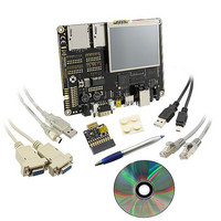
BMSKTOPASA900(DCE) Toshiba, BMSKTOPASA900(DCE) Datasheet - Page 368

BMSKTOPASA900(DCE)
Manufacturer Part Number
BMSKTOPASA900(DCE)
Description
KIT STARTER TMPA900 USB JTAG
Manufacturer
Toshiba
Series
TOPASr
Type
MCUr
Specifications of BMSKTOPASA900(DCE)
Contents
Evaluation Board, Cable(s), Software and Documentation
For Use With/related Products
TMPA900CMXBG
Lead Free Status / RoHS Status
Lead free / RoHS Compliant
- Current page: 368 of 959
- Download datasheet (5Mb)
3.13.1.1 Operation Description
Note:The number of STOP bit can be selected as 1 bit or 2 bits by setting UARTxLCR_H<STP2>. The term STOP bit
(1) Baud rate generator
(2) Transmit FIFO
(3) Receive FIFO
(4) Transmit logic
(5) Receive logic
(6) Interrupt generation logic
(7) Interrupt timing
here means the last STOP bit.
The transmit FIFO is an 8-bit wide, 16-location deep, FIFO memory buffer. CPU data
written across the APB interface is stored in the FIFO until it is read out by the
transmit logic. You can disable the transmit FIFO to act like a one-byte holding
register.
The receive FIFO is a 12-bit wide, 16 locations deep, FIFO memory buffer. Received
data and corresponding error bits are stored in the receive FIFO by the receive logic
until they are read out by the CPU across the APB interface. The receive FIFO can be
disabled to act like a one-byte holding register.
The transmit logic performs parallel-to-serial conversion on the data read from the
transmit FIFO. Control logic outputs the serial bit stream beginning with a start bit,
data bits with the Least Significant Bit (LSB) first, followed by the parity bit, and then
the stop bits according to the programmed configuration in control registers.
The receive logic performs serial-to-parallel conversion on the received bit stream after
a start bit has been detected. Error check for overrun, parity and frame and line break
detection are also performed. Their error bit data is written to the receive FIFO.
timing of UART transmit and receive, and the internal IrLPBaud16 circuit which
generates the pulse width of the IrDA encoded transmit bit stream when in low-power
mode.
UART outputs a maskable combined interrupt for every interrupt sources.
The baud rate generator contains the internal Baud16 clock circuit which controls the
Overrun error
Break error
Parity error
Frame error
Receive timeout error
Transmit interrupt
Receive interrupt
Interrupt type
TENTATIVE
After receiving the stop bit of Overflow data
After receiving STOP bit
After receiving parity data
After receiving frame over bit
After 511 clocks (Baud16) from Receive FIFO data storage.
After transmitting the last data (MSB data).
After receiving STOP bit
TMPA900CM- 367
Interrupt timing
TMPA900CM
2009-10-14
Related parts for BMSKTOPASA900(DCE)
Image
Part Number
Description
Manufacturer
Datasheet
Request
R
Part Number:
Description:
Toshiba Semiconductor [TOSHIBA IGBT Module Silicon N Channel IGBT]
Manufacturer:
TOSHIBA Semiconductor CORPORATION
Datasheet:
Part Number:
Description:
TOSHIBA GTR MODULE SILICON NPN TRIPLE DIFFUSED TYPE
Manufacturer:
TOSHIBA Semiconductor CORPORATION
Datasheet:
Part Number:
Description:
TOSHIBA GTR Module Silicon N Channel IGBT
Manufacturer:
TOSHIBA Semiconductor CORPORATION
Datasheet:
Part Number:
Description:
TOSHIBA Intelligent Power Module Silicon N Channel IGBT
Manufacturer:
TOSHIBA Semiconductor CORPORATION
Datasheet:
Part Number:
Description:
TOSHIBA INTELLIGENT POWER MODULE SILICON N CHANNEL LGBT
Manufacturer:
TOSHIBA Semiconductor CORPORATION
Datasheet:
Part Number:
Description:
TOSHIBA IGBT Module Silicon N Channel IGBT
Manufacturer:
TOSHIBA Semiconductor CORPORATION
Datasheet:
Part Number:
Description:
TOSHIBA GTR MODULE SILICON N−CHANNEL IGBT
Manufacturer:
TOSHIBA Semiconductor CORPORATION
Datasheet:
Part Number:
Description:
TOSHIBA Intelligent Power Module Silicon N Channel IGBT
Manufacturer:
TOSHIBA Semiconductor CORPORATION
Datasheet:
Part Number:
Description:
TOSHIBA GTR Module Silicon N Channel IGBT
Manufacturer:
TOSHIBA Semiconductor CORPORATION
Datasheet:
Part Number:
Description:
TOSHIBA INTELLIGENT POWER MODULE
Manufacturer:
TOSHIBA Semiconductor CORPORATION
Datasheet:
Part Number:
Description:
TOSHIBA Intelligent Power Module Silicon N Channel IGBT
Manufacturer:
TOSHIBA Semiconductor CORPORATION
Datasheet:
Part Number:
Description:
TOSHIBA Intelligent Power Module Silicon N Channel IGBT
Manufacturer:
TOSHIBA Semiconductor CORPORATION
Datasheet:
Part Number:
Description:
TOSHIBA IGBT Module Silicon N Channel IGBT
Manufacturer:
TOSHIBA Semiconductor CORPORATION
Datasheet:
Part Number:
Description:
TOSHIBA Intelligent Power Module Silicon N Channel IGBT
Manufacturer:
TOSHIBA Semiconductor CORPORATION
Datasheet:
Part Number:
Description:
Toshiba Semiconductor [SILICON N CHANNEL 1GBT]
Manufacturer:
TOSHIBA Semiconductor CORPORATION
Datasheet:


