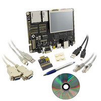
BMSKTOPASA900(DCE) Toshiba, BMSKTOPASA900(DCE) Datasheet - Page 430

BMSKTOPASA900(DCE)
Manufacturer Part Number
BMSKTOPASA900(DCE)
Description
KIT STARTER TMPA900 USB JTAG
Manufacturer
Toshiba
Series
TOPASr
Type
MCUr
Specifications of BMSKTOPASA900(DCE)
Contents
Evaluation Board, Cable(s), Software and Documentation
For Use With/related Products
TMPA900CMXBG
Lead Free Status / RoHS Status
Lead free / RoHS Compliant
- Current page: 430 of 959
- Download datasheet (5Mb)
[31:8]
[7:0]
[31:8]
[7:0]
[Description]
a. <DB[7:0]>
Bit
Bit
Note:
Note: In receive mode, if data is written to I2C0DBR before the received data is read out, the received data will be
2.
aligned on the left side.
right side.
written to I2C0DBR<DB[7:1]> and the transfer direction is specified in I2C0DBR<DB[0]>
as follows:
dedicated transmit buffer in transmit mode and as a dedicated receive buffer in receive
mode. This register should be accessed on a transfer-by-transfer basis.
on the bus.
internal interrupt after the current transfer and initiates the next transfer.
These bits are used to store data for serial transfer.
When this module is a transmitter, the data to be transmitted is written into DB[7:0]
When this module is a receiver, the received data is stored into DB[7:0] aligned on the
When the master needs to transmit a slave address, the transfer target address is
0y0: Master (transmission) → Slave/reception
0y1: Master (reception) ← Slave/transmission
When all the bits in the I2C0DBR register are written as 0, a general call can be sent out
In both transmission and reception modes, a write to the I2C0DBR register releases the
Although I2C0DBR is provided as a transmit/receive buffer, it should be used as a
I2C0DBR (I
corrupted.
This register is initialized only after a hardware reset. It is not initialized by a software reset. (The most recent
data is retained.)
−
DB[7:0]
−
DB[7:0]
Bit Symbol
Bit Symbol
2
C0 Data Buffer Register)
−
RO
−
WO
Type
Type
TENTATIVE
TMPA900CM- 429
Undefined
0x00
Undefined
0x00
Reset
Reset
Value
Value
Read as undefined.
Read: Receive data is read (Note)
Read as undefined. Write as zero.
Write: Transmit data is written (Note)
Address = (0xF007_0000) + (0x0004)
Address = (0xF007_0000) + (0x0004)
Description
Description
TMPA900CM
2009-10-14
Related parts for BMSKTOPASA900(DCE)
Image
Part Number
Description
Manufacturer
Datasheet
Request
R
Part Number:
Description:
Toshiba Semiconductor [TOSHIBA IGBT Module Silicon N Channel IGBT]
Manufacturer:
TOSHIBA Semiconductor CORPORATION
Datasheet:
Part Number:
Description:
TOSHIBA GTR MODULE SILICON NPN TRIPLE DIFFUSED TYPE
Manufacturer:
TOSHIBA Semiconductor CORPORATION
Datasheet:
Part Number:
Description:
TOSHIBA GTR Module Silicon N Channel IGBT
Manufacturer:
TOSHIBA Semiconductor CORPORATION
Datasheet:
Part Number:
Description:
TOSHIBA Intelligent Power Module Silicon N Channel IGBT
Manufacturer:
TOSHIBA Semiconductor CORPORATION
Datasheet:
Part Number:
Description:
TOSHIBA INTELLIGENT POWER MODULE SILICON N CHANNEL LGBT
Manufacturer:
TOSHIBA Semiconductor CORPORATION
Datasheet:
Part Number:
Description:
TOSHIBA IGBT Module Silicon N Channel IGBT
Manufacturer:
TOSHIBA Semiconductor CORPORATION
Datasheet:
Part Number:
Description:
TOSHIBA GTR MODULE SILICON N−CHANNEL IGBT
Manufacturer:
TOSHIBA Semiconductor CORPORATION
Datasheet:
Part Number:
Description:
TOSHIBA Intelligent Power Module Silicon N Channel IGBT
Manufacturer:
TOSHIBA Semiconductor CORPORATION
Datasheet:
Part Number:
Description:
TOSHIBA GTR Module Silicon N Channel IGBT
Manufacturer:
TOSHIBA Semiconductor CORPORATION
Datasheet:
Part Number:
Description:
TOSHIBA INTELLIGENT POWER MODULE
Manufacturer:
TOSHIBA Semiconductor CORPORATION
Datasheet:
Part Number:
Description:
TOSHIBA Intelligent Power Module Silicon N Channel IGBT
Manufacturer:
TOSHIBA Semiconductor CORPORATION
Datasheet:
Part Number:
Description:
TOSHIBA Intelligent Power Module Silicon N Channel IGBT
Manufacturer:
TOSHIBA Semiconductor CORPORATION
Datasheet:
Part Number:
Description:
TOSHIBA IGBT Module Silicon N Channel IGBT
Manufacturer:
TOSHIBA Semiconductor CORPORATION
Datasheet:
Part Number:
Description:
TOSHIBA Intelligent Power Module Silicon N Channel IGBT
Manufacturer:
TOSHIBA Semiconductor CORPORATION
Datasheet:
Part Number:
Description:
Toshiba Semiconductor [SILICON N CHANNEL 1GBT]
Manufacturer:
TOSHIBA Semiconductor CORPORATION
Datasheet:


