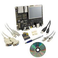
BMSKTOPASA900(DCE) Toshiba, BMSKTOPASA900(DCE) Datasheet - Page 955

BMSKTOPASA900(DCE)
Manufacturer Part Number
BMSKTOPASA900(DCE)
Description
KIT STARTER TMPA900 USB JTAG
Manufacturer
Toshiba
Series
TOPASr
Type
MCUr
Specifications of BMSKTOPASA900(DCE)
Contents
Evaluation Board, Cable(s), Software and Documentation
For Use With/related Products
TMPA900CMXBG
Lead Free Status / RoHS Status
Lead free / RoHS Compliant
- Current page: 955 of 959
- Download datasheet (5Mb)
4.4
Analog reference voltage (+)
Analog reference voltage (−)
AD converter power supply voltage
AD converter GND
Analog input voltage
Analog reference voltage
Power supply current
Full Scale Error
Offset Error
Differential Error
Integral Error
AD Conversion Characteristics
Note: “Caltulation” of following table is effective in a range of AVCC3AD = 3.0V to 3.6V, DVCC1A = DVCC1B =
Parameter
Note 1: Error = (“conversion result” – “theoretical value”)
Note 2: The quantization error does not include.
Note 3: Minimum operating frequency
DVCC1C = 1.4 to 1.6V.
1 LSB = (VREFH − VREFL)/1024[V]
The minimum operating clock and maximum operating clock (ADCLK) of the AD converter is 3 MHz and 33
MHz, respectively. (3MHz ≤ ADCLK ≤ 33MHz)
Minimum conversion time is 1.39μs at 33MHz, and maximum conversion time is 15.3μs at 3MHz.
AVCC3AD
IREFOFF
Symbol
IREFON
VREFH
VREFL
EFULL
AVSS
EOFF
EDNL
AVIN
EINL
TMPA900CM- 954
TENTATIVE
<VREFON> = 1
<VREFON> = 0
Condition
DVSSCOMn
DVSSCOMn
AVCC3AD
VREFL
Min
3.0
DVSSCOMn
DVSSCOMn
AVCC3AD
-1 to +2
-2 to +3
Typ
3.3
2.1
0.1
+1
‐3
DVSSCOMn
DVSSCOMn
AVCC3AD
VREFH
-1 to +4
-4 to +1
Max
3.6
3.5
10
±2
±3
TMPA900CM
2009-10-14
Unit
LSB
LSB
LSB
LSB
mA
μA
V
Related parts for BMSKTOPASA900(DCE)
Image
Part Number
Description
Manufacturer
Datasheet
Request
R
Part Number:
Description:
Toshiba Semiconductor [TOSHIBA IGBT Module Silicon N Channel IGBT]
Manufacturer:
TOSHIBA Semiconductor CORPORATION
Datasheet:
Part Number:
Description:
TOSHIBA GTR MODULE SILICON NPN TRIPLE DIFFUSED TYPE
Manufacturer:
TOSHIBA Semiconductor CORPORATION
Datasheet:
Part Number:
Description:
TOSHIBA GTR Module Silicon N Channel IGBT
Manufacturer:
TOSHIBA Semiconductor CORPORATION
Datasheet:
Part Number:
Description:
TOSHIBA Intelligent Power Module Silicon N Channel IGBT
Manufacturer:
TOSHIBA Semiconductor CORPORATION
Datasheet:
Part Number:
Description:
TOSHIBA INTELLIGENT POWER MODULE SILICON N CHANNEL LGBT
Manufacturer:
TOSHIBA Semiconductor CORPORATION
Datasheet:
Part Number:
Description:
TOSHIBA IGBT Module Silicon N Channel IGBT
Manufacturer:
TOSHIBA Semiconductor CORPORATION
Datasheet:
Part Number:
Description:
TOSHIBA GTR MODULE SILICON N−CHANNEL IGBT
Manufacturer:
TOSHIBA Semiconductor CORPORATION
Datasheet:
Part Number:
Description:
TOSHIBA Intelligent Power Module Silicon N Channel IGBT
Manufacturer:
TOSHIBA Semiconductor CORPORATION
Datasheet:
Part Number:
Description:
TOSHIBA GTR Module Silicon N Channel IGBT
Manufacturer:
TOSHIBA Semiconductor CORPORATION
Datasheet:
Part Number:
Description:
TOSHIBA INTELLIGENT POWER MODULE
Manufacturer:
TOSHIBA Semiconductor CORPORATION
Datasheet:
Part Number:
Description:
TOSHIBA Intelligent Power Module Silicon N Channel IGBT
Manufacturer:
TOSHIBA Semiconductor CORPORATION
Datasheet:
Part Number:
Description:
TOSHIBA Intelligent Power Module Silicon N Channel IGBT
Manufacturer:
TOSHIBA Semiconductor CORPORATION
Datasheet:
Part Number:
Description:
TOSHIBA IGBT Module Silicon N Channel IGBT
Manufacturer:
TOSHIBA Semiconductor CORPORATION
Datasheet:
Part Number:
Description:
TOSHIBA Intelligent Power Module Silicon N Channel IGBT
Manufacturer:
TOSHIBA Semiconductor CORPORATION
Datasheet:
Part Number:
Description:
Toshiba Semiconductor [SILICON N CHANNEL 1GBT]
Manufacturer:
TOSHIBA Semiconductor CORPORATION
Datasheet:


